Home > Analog CMOS Design > MOSFET Amplifiers > Common Source Amplifier
Common Source Amplifier :
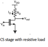
Figure below shows the common source amplifier circuit. In this circuit the MOSFET converts variations in the gate-source voltage into a small signal drain current which passes through a resistive load and generates the amplified voltage across the load resistor.
Now from above Figure,

Also, from small signal model of shown in above Figure.
By applying KVL,
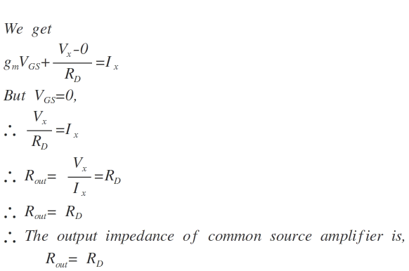
In order to calculate the output impedance Rout consider the
circuit shown in
Figure below.
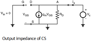
By applying KCL at point 'A'
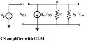
If we consider the non Ideal effect such as channel length modulation in
the CS amplifier then the small signal model includes one more resistor
i.e. ro as shown in
Figure below.
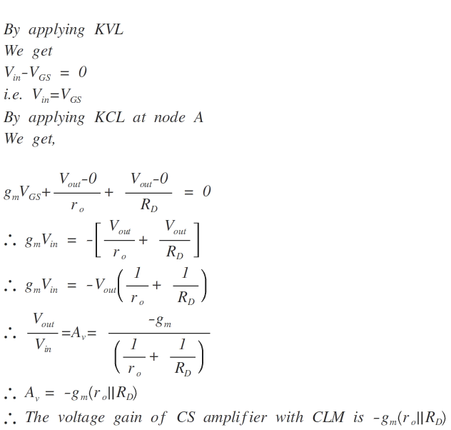
The current gain and input impedance will not be affected by CLM and theses are Ai = ¥ and Rin = ¥. But the output impedance is affected because of CLM.
In order to calculate the output impedance of CS amplifier with CLM consider the circuit as shown in Figure below.
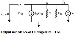
By applying KCL at node 'A'
We get, gm VGS + + = Ix
\ Vx = Ix [ VGS = Vin = 0]
\ =
\ Rout = (ro || RD)
Thus, the output impedance of the CS amplifier with CLM is ro || R D.
In order to derive the voltage gain of CS amplifier with CLM using I-V characteristics consider the drain current equation with CLM as :
IDS = mn Cox (VGS - V TH)2 (1 + l VDS)
where l is channel length modulation coefficient.
From Fig. 8.9.1(a)
VDD - IDRD = Vout
\ Vout = VDD - mn Cox (V in - VTH)2 (1 + l Vout)
Differentiating this equation with respect to Vin.
By product rule of differentiation :
= - mn Cox (Vin - VTH) 2
- mn Cox (1 + l Vout) ´ 2 (Vin - VTH)
An = - mn Cox (Vin - VTH)2 An - gm R D
By approximating ID as :
ID = mn Cox (Vin - V TH)2
We get, An = - gm RD - RD × l × ID × An
\ An(1 + RD × l ID) = - g m RD
\ An =
As we know that ro is the linear resistor given as :
ro =
To obtain the value of this resistor differentiating ID with respect to VDS,
\ ID = mn Cox (VGS - V TH)2 (1 + l VDS)
= mn Cox (VGS - VTH) 2 (l)
\ Approximating ID we get,
\ = l ID
\ An = =
i.e. An = - gm (ro || RD)
which is same as the voltage gain derived using small signal model.
Thus, the voltage gain of CS amplifier is depends upon the transconductance gm, the linear resistor ro and load. In order to increase the gain we have to increase the gm. Inturn we have to increase the ratio.
Hence the gain of amplifier is increases with increasing 'W' and decreasing 'L'. The ro resistance is appears in shunt with RD because of this the effect of ro (i.e. channel length modulation) decreases the voltage gain of amplifier on the other hand the effect of parallel combination of ro and RD decreases the output impedance (R out) which is the beneficial effect.
In order to increase the gain of the amplifier along with gm another important factor is the load impedance connected at the output. To have larger gain load impedance should be larger. The two choices of load impedance of CS stages are :
1) Current source load
2) Diode connected load.