Home > Analog CMOS Design > MOSFET Amplifiers > PMOS Load Inverter
PMOS Load Inverter :
Figure below shows the circuit diagram of the PMOS load inverter.
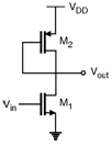
Figure below shows the input output characteristics of the PMOS load inverter. The output voltage equals VDD - VTH2 if V in < VTH1.
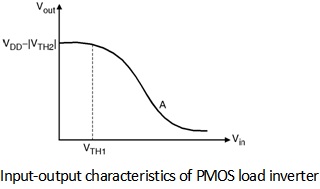
For Vin > VTH1 Vout follower an approximately straight line. As Vin exceeds Vout + V TH1 i.e. beyond point A M1 enters in the triode region and the characteristics becomes non linear.