Home > Digital CMOS Design > MOS Capacitor > Band Diagram of Ideal MOS
Band Diagram of Ideal MOS Structure at Equilibrium
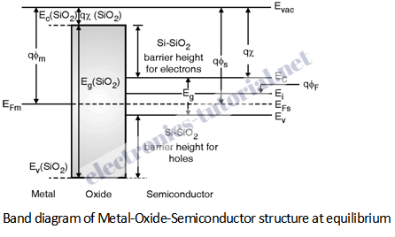
Let us assume that the metal and semiconductor have identical work functions. We start drawing the band diagram by aligning the metal and the semiconductor fermi levels i.e. EFm and EFs. Then we draw the vacuum level Evac, which is equidistant from both EFs and EFm, since we have assumed that the metal and the semiconductor have identical work function. Now we are in a position to draw the band diagram of oxide with its conduction band lying bellow the vacuum level by an amount equal to the electron affinity of oxide which is to be equal to 0.9 eV and the valence band lying bellow the conduction band by an amount equal to the band gap energy of oxide which is roughly equal to 9 eV. Now we can draw the intrinsic level Ei as per the substrate doping. Here, for p-type substrate Ei is above EF by the energy qΦF where ΦF is the bulk potential. For p-type substrate with doping concentration NA bulk potential is expressed as,
ΦF = VT * Ln (NA / ni )
where VT = KT/q is thermal voltage.
Once the location of Ei is known the conduction and valence bands can be easily drawn. This completes the construction of the band diagram, at equilibrium. Figure below shows the complete band diagram of the MOS structure at equilibrium.