At high frequencies the gain of the ideal differentiator is very high. This high gain makes the circuit unstable. Thus to avoid this resistance Rc is added in series with capacitor C and a capacitor Cc is added in parallel with resistance R.
The practical differentiator is shown below.

Here Rc and Cc are called as compensating components.
Input source loading is avoided through Rc though C gets shorted. At high frequency, the reactance of Cc is small so high frequency noise gets bypassed and not appeared at output.
Frequency response of practical differentiator:
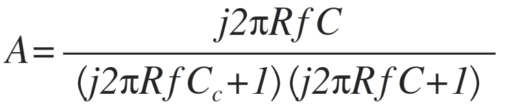
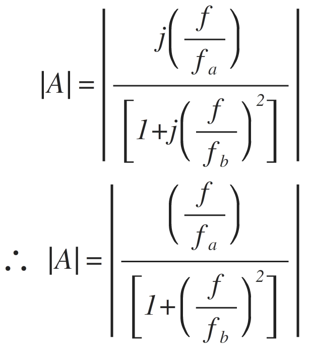
The gain of the practical differentiator can be calculated as
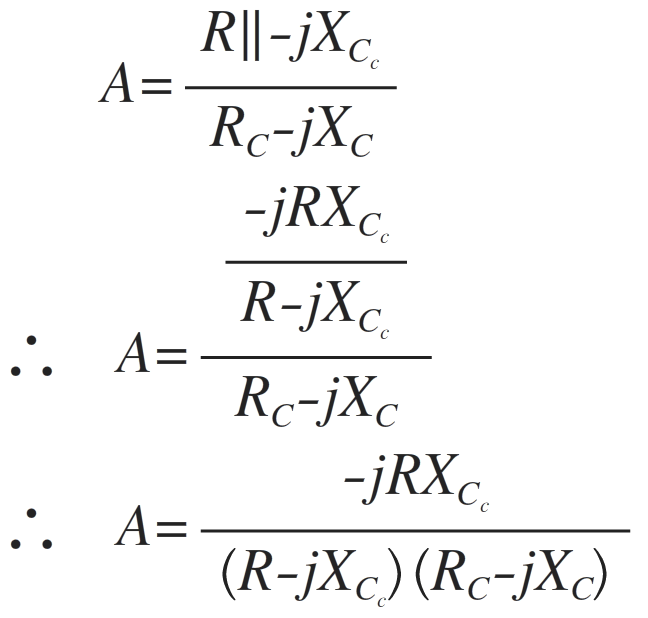
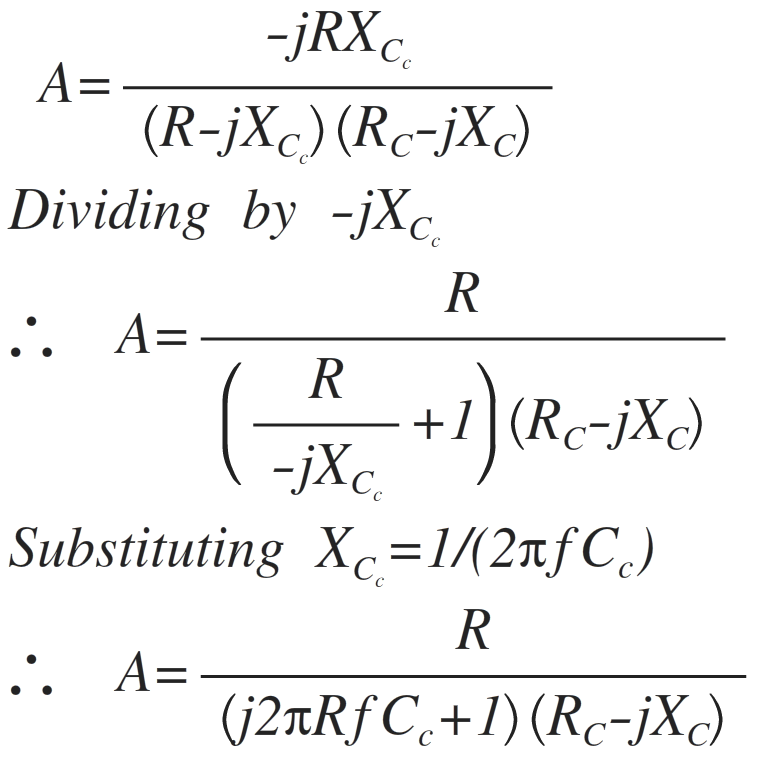
Divide Numerator and Denominator by -jXc

Substituting Xc=1/2πfC
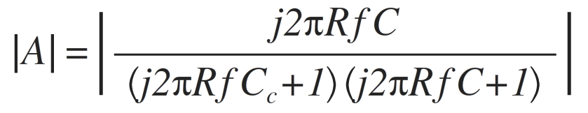
The magnitude of gain A is
From the ideal differentiator, the 0 dB frequency fa is given as
f_a=1/2πRC
Let assume the frequency fb as
fb=1/(2πRCc )
Since RCC = RCC we get
f_b=1/(2πRCc )=1/(2πRc C)
Substituting the values of frequencies fa and fb , the gain A is
The following figure shows the frequency response curve for practical differentiator.
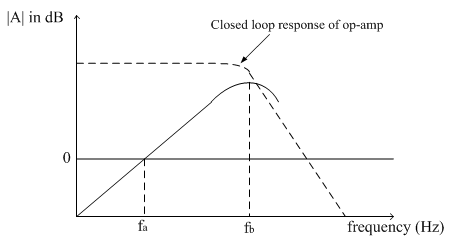
Select RC, C, R and CCsuch that the response cuts the actual response of the closed loop configuration of op-amp
Within the frequency range fa to fb the response is highly linear and hence referred as true differentiation range. Thus fb should be selected as high as possible as fa. The selection of frequencies should be in the following way fa<fb<fc
where fc=≫unity gain bandwidth of op-amp
Design procedure for practical differentiator:
Select fa as the highest frequency of input signal.
Assume C and calculate R from the equation fa=1/2πRC
Select fb ≥ 10fa and calculate RC and CC so that RC.C = R.CC