Home > mini projects > 2 Bit Parallel or Flash Analog to Digital Converter
2-Bit Parallel or Flash Analog to Digital Converter
Abstract -A 2 bit parallel analog to digital converter using comparators and priority encoder giving digital output is proposed, designed, and implemented using transistor-transistor logic . The circuit is found to be working satisfactorily . this is also called as flash ADC.
I. Introduction
» An analog-to-digital converter (A/D or ADC) produces a digital number corresponding to an analog input voltage sample.
» Flash ADC Consists of a series of comparators, each one comparing the input signal to a unique reference voltage.
» The comparator outputs connect to the inputs of a priority encoder circuit, which produces a binary output
II. Design and Working
Input voltage 0-5v. Output -2 bit binary. Any input voltage between 0-5v will be converted into corresponding binary output.
The circuit shown in figure takes the given analog signal as input (varying from 0-5v) and produces a digital output corresponding to the input given. In this circuit ,we used three comparators and a 4*2 priority encoder. There are four resistors of equal value of 1kohm each. And the reference voltage is taken as 5volts.
A. According to voltage division rule, the reference voltage given is divided into 3Vr/4 ,2Vr/4, Vr/4 at posituve terminal of the comparators respectively. Here, 'Vr' is the reference voltage. Span is defined as the difference between maximum and minimum analog input voltages and here, it is 5v. step size is given by span/2^n where n is number of bits in the binary output(here, n=2). Hence, stepsize is 5/4=1.25 (here).
B. Now, the negative terminals of the comparators are given the input voltage as analog signal and by comaparing the positive and negative terminals, as the analog input voltage exceeds the reference voltage at each comparator, the comparator outputs will go to a high state. By considering first comparator, the negative terminal has input voltage 'Va' and the positive terminal has input as '3Vr/4' . if Va is greater than 3Vr/4, the output will be logic 1; else the output will be logic 0. Similarly, the same procedure is repeated for the remaining comparators with their respective reference voltages.
C. The outputs of comparators are given as inputs to the priority encoder and the corresponding binary outputs are generated. The priority encoder generates a binary number based on the highest-order active input, ignoring all other active inputs. The output of the first comparator will be higher priority input compared to other bits.
III. ADVANTAGES
Simplest of all analog to digital converters. Most efficient in terms of speed, very fast; limited only in terms of comparator and gate propagation delays.
IV. INPUT RANGES AND CORRESPONDING OUTPUT
|
Input values |
Output |
|
0-1.25 |
00 |
|
1.25-2.5 |
01 |
|
2.5-3.75 |
10 |
|
3.75-5 |
11 |
V. CIRCUIT DIAGRAM
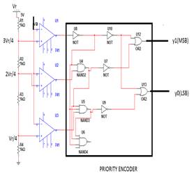
Fig 1
VI. Figures and Results
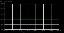
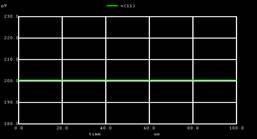
The output of priority encoder corresponding to different inputs :
A. Input=5v, output=11
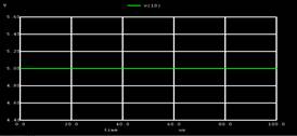
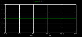
B. Input=3v, output =10
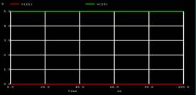
C. Input=2v, output=01
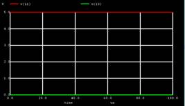
D. Input=1v, output=00
VII. CODES
*analog to digital
.include opamp.cir
.include spe.cir
r1 1 2 1k
r2 2 3 1k
r3 3 4 1k
r4 4 0 1k
x1 5 2 6 opamp
x2 5 3 7 opamp
x3 5 4 8 opamp
x4 6 7 8 9 10 11 prior
vr 1 0 dc 5
va 5 0 dc 1
v1 9 0 dc 5
.tran 1u 100us
.control
run
display
plot v(10)
plot v(11)
set xbrushwidth=3
.endc
.end
SUBCIRCUITS :
*priority encoder
.subckt prior 1 3 5 7 11 12
.include snot.cir
.include ors.cir
.include nand.cir
.include subnand3.cir
x1 1 2 not
x2 2 3 4 nand1
x3 4 2 5 6 nand3
x4 4 9 not
x5 6 10 not
x6 1 9 11 or
x7 1 10 12 or
.ends prior
*opamp
.subckt opamp 1 2 6
r1 1 2 10meg
e1 3 0 1 2 100k
r2 3 4 1k
c1 4 0 15u
e2 5 0 4 0 1
r3 5 6 10
.ends opamp
*not
.subckt not 1 3
.model mosfet1 pmos
.model mosfet2 nmos
m1 3 1 2 2 mosfet1
m2 3 1 0 0 mosfet2
vdd 2 0 dc 5
.ends not
*2 input nand
.subckt nand1 2 3 4
.model mos1 pmos
.model mos2 nmos
m1 4 2 1 1 mos1
m2 4 3 1 1 mos1
m3 4 2 5 0 mos2
m4 5 3 0 0 mos2
v1 1 0 dc 5
.ends nand1
*3 input nand
.subckt nand3 1 2 3 6
.include nand.cir
x1 1 2 4 nand1
x2 4 4 5 nand1
x3 5 3 6 nand1
.ends nand3
*or gate
.subckt or 1 3 5
.include nand.cir
x1 1 1 2 nand1
x2 3 3 4 nand1
x3 2 4 5 nand1
.ends or