Home > mini projects > DC boost circuit using 555 timer
DC Boost Circuit using 555 Timer
Abstract - Different devices used in day-to-day life demand different voltage levels for their proper working. To fulfill these voltage requirements, circuits need to be designed which can convert available voltage levels into desired ones. In this project, we propose a DC boost circuit using 555 timer. The circuit amplifies the input voltage levels to required voltage level by adjusting the gain. This is achieved by using suitable component values.
Index Terms -DC boost; 555 timer.
I. INTRODUCTION
DC boost circuit has applications in many electronic devices requiring voltage amplification. The circuit enhances the DC level of voltage supply thereby enabling the user to have two different voltage levels. Depending on the values of the internal components used, the same circuit can be designed for attenuation as well as amplification of voltage levels. The DC boost circuit takes a pulse input as provided by the 555 timer IC (0V-5V) in astable mode and produces the amplified pulse at the output.
II. WORKING
The proposed DC boost circuit is designed using 555 timer IC in astable mode and operational amplifier in non-inverting mode. The 555 timer IC generates an output pulse (0V-5V) which is given as an input to the operational amplifier. The operational amplifier works in the non-inverting mode and produces an amplified output pulse without introducing any phase shift.
III. 555 TIMER
555 timer IC is one of the most widely used ICs in electronics. It consists of three internal resistors forming a voltage divider, two comparators and a S-R flip-flop. It has three modes of operation; namely monostable, bistable and astable mode. It works as a 1-Short pulse generator in monostable mode, as an oscillator in astable mode and produces a flip-flop type action in bistable mode Pin description of timer 555 IC:
Pin 1 : Ground
Pin2 : Trigger : This pin is connected to the negative input of comparator 2.
Pin3: Output : Load is connected at this pin. It can be used as source or sink and can drive upto 200mA current.
Pin 4: Reset : This is active low pin connected to the master reset of flip-flop in timer chip. It is normally connected to Vcc for preventing accidental reset.
Pin 5: Control Voltage : Voltage provided at this pin can control the pulse width of the output irrespective of the RC network. It is grounded through a capacitance to avoid noise. Pin 6: Threshold : Voltage at this pin determines when to reset the flip-flop.
Pin 7: Discharge : This pin is drawn from the open collector of transistor. Whenever output pin goes low, the discharge pin is pulled to ground and the capacitor discharges. Pin 8: Vcc.
The voltage divider configuration provides a fixed voltage of (2Vcc/3) at the inverting terminal of comparator 1 and (Vcc/3) at the non-inverting terminal of comparator 2. Capacitor is initially discharged and voltage across it is 0V. The non-inverting terminal of comparator 1 and the inverting terminal of comparator 2 are shorted and have voltage same as the voltage across capacitor (Vc). Base of npn transistor is connected to Q' and is ON whenever Q'=1
Following cases arise :
1) Vc < Vcc/3 : R=0 , S=1, Q =1, Q'=0
Transistor will be off. Capacitor charges through Ra and Rb.
2)Vcc/3 <Vc < 2Vcc/3 : R=0 , S=0, Output of flip-flop remains in the previous state .So transistor will be off. Capacitor continues to charge through Ra and Rb.
3) Vc > 2Vcc/3 : R=1 , S=0, Q =0, Q'=1
Transistor will be on. Capacitor discharges through Rb.
Charging time = Ton= (Ra+Rb)Cln(2)
Discharging time = Toff = (Rb)Cln(2)
Total time = Ton+ Toff = (Ra+2Rb)Cln(2)
|
Duty Cycle = |
= |
+ |
||
|
+ |
+2 |
|||
IV. OP-AMP
Operational amplifier is a three terminal device with two inputs as inverting, non-inverting and a single ended output. It is used for ideal DC amplification. It works in two configurations namely inverting and non-inverting. In this project op-amp is used in its non-inverting mode, where the input is given to non-inverting terminal of op-amp.
Gain of op-amp in non-inverting mode = 1+ 2 1
![]()
As seen from above equation, gain can be varied by changing the values of R2 and R1.
V. DESIGN
The following sub-circuits have been used in designing the DC Boost circuit.
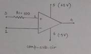
Comparator sub-circuit:
.subckt comp 3 1 4
.include op1.cir
x1 2 1 5 6 4 opamp
r1 3 2 100 vcc 5 0 5 vee 6 0 -5
.ends comp_sub
Not-gate sub-circuit:
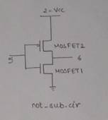
.subckt not 5 6
.model MOSFET1 nmos .model MOSFET2 pmos M1 6 5 2 4 MOSFET2 M2 6 5 0 0 MOSFET1 vdd 2 0 dc 5v v1 4 0 dc 5v
.ends not_sub
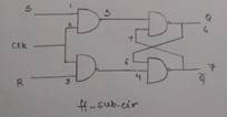
Flip-flop sub-circuit:
.subckt ff 1 3 2 6
.include nand_sub1.cir
x1 1 2 5 nand
x2 2 3 4 nand
x3 5 7 6 nand
x4 4 6 7 nand
.ends ff_sub
555 IC sub-circuit:
.subckt ic 1 3 2 4 12 8
.include ff_sub.cir
.include not_sub.cir
.include comp_sub.cir
.model bjt npn
.model bjt1 pnp x1 7 6 11 8 ff x2 3 4 6 comp
x3 5 3 7 comp
x4 8 9 not
q1 2 10 0 bjt
q2 9 12 1 bjt1
r1 1 4 5k
r2 4 5 5k
r3 5 0 5k
r4 9 10 100k
vclk 11 0 pulse(0 5 0 0 0 2u 4u)
.ends
Op-amp sub-circuit:
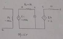
.subckt opamp 1 2 6 E1 3 0 2 1 100k E2 5 0 4 0 1 R1 1 2 1meg
r2 3 4 1k
r3 5 6 10
c1 4 0 1.6u
.ends opamp
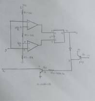
Op-amp (with power supply) sub-circuit:
.subckt opamp 1 2 3 4 5
|
c1 |
11 |
12 8.661E-12 |
|
c2 |
6 |
7 30.00E-12 |
|
dc |
5 53 dx |
|
|
de |
54 |
5 dx |
dlp 90 91 dx
dln 92 90 dx
Dp 4 3 dx
egnd 99 0 poly(2) (3,0) (4,0) 0 .5 .5
fb 7 99 poly(5) vb vc ve vlp vln 0 10.61E6 -10E6 10E6 10E6 -10E6
Ga 6 0 11 12 188.5E-6
Gcm 0 6 10 99 5.961E-9
iee 10 4 dc 15.16E-6
hlim 90 0 vlim 1K
q1 11 2 13 qx
q2 12 1 14 qx
r2 69 100.0E3
rc13 11 5.305E3
rc2 3 12 5.305E3
re1 13 10 1.836E3
re2 14 10 1.836E3
ree 10 99 13.19E6
|
ro1 |
8 5 50 |
|
|
ro2 |
7 |
99 100 |
|
rp |
3 |
4 18.16E3 |
|
vb |
9 0 dc 0 |
|
|
vc |
3 53 dc 1 |
|
|
ve |
54 4 dc 1 |
|
vlim 7 8 dc 0
vlp 91 0 dc 40
vln 0 92 dc 40
.model dx D(Is=800.0E-18 Rs=1)
.model qx NPN(Is=800.0E-18 Bf=93.75)
.ends
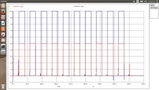
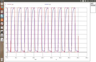
The following waveforms were obtained as the output of 555 timer and DC Boost circuit.
555 Timer IC output : red
DC boost circuit output : blue
555 Timer IC output : red
Voltage across capacitor : blue
DC boost circuit was implemented using 555 timer and op-amp in non-inverting configuration. The threshold and trigger pins are shorted in astable mode.The frequency of output pulse of 555 timer can be varied by changing the values of resistances connected between Vcc and Discharge Pin, Discharge and Threshold pin and the capacitor between threshold and ground. The output of 555 timer (0V-5V) was amplified using appropriate values of resistors connected to op-amp (R1 and R2). Thus a simplified DC boost circuit was implemented.