Home > mini projects > Design and Phase Frequency Detector Using Different Logic Gates in CMOS Process Technology
Design and Implementation of Phase Frequency Detector Using Different Logic Gates in CMOS Process Technology
Abstract - The Phase Detectors determines the relative phase difference between the two incoming signals and outputs a signal that is proportional to this phase difference. The phase detector also detects the frequency error; they are called Phase Frequency Detectors (PFD). It is very important block for the Clock and Data Recovery circuit. This project presents the different design schemes of the PFD and compares them with their output results. The circuits that have been considered are the PFD using NAND Gate, PFD using NOR Gate and PFD using AND Gate. The PFD is implemented with True Single Phase Clocked logic. The different PFD circuits are designed and simulated on NG Spice Tool using CMOS process technology with supply voltage 1 V.
I.INTRODUCTION
The rapid growth in wireless applications in last decade has motivated to design fully integrated, low power, low cost and high performance transceivers. The Clock and Data Recovery circuit is most importance in wireless communication device which is useful to generate clock and recover the data. Clock and Data Recovery finds wide application in the area such as Serial data communication, Repeater, satellite communication, optical transceiver, chip to chip interconnects etc.
PFD in PLL is used to detect the phase as well as frequency difference between the two signals that is reference signal and the output from VCO as compared to the phase detectors which are capable of detecting the phase difference only. The characteristics of PFD have huge impact on performance of PLL. The lock time and timing jitter of a PLL are largely affected by the characteristics of phase frequency detector.[Refer fig.1]
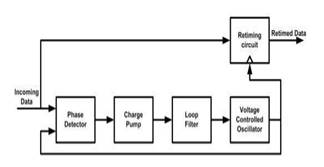
Fig. 1 Clock and Data Recovery circuit
II. CIRCUITS ARCHITECTURE
A.NAND Gate Based PFD
The circuit consists of two resettable, edge triggered D flip flops with their D inputs tied to logic 1 and a NAND Gate in the reset path(fig.2). The explanation of the general operation of the PFD begins by describing the initial state of the device. First, the UP and DN signals are reset to low or zero and assume both the Ref frequency signal and the Div signal are high or one. Additionally, the Ref frequeny waveform is slightly leading the Div waveform, hence as falling edge occurs on the Ref input, the high or one on the D input is transmitted to the Q output or UP.Short time later, the Div waveform experience a falling edge and the Q output or DN of the other flip lop is set. Once both UP and DN are high or ONE, the NAND gate experiences a transition to force the Reset signal to zero. The flip flops are designed so that zeros on the Reset signal resets the Q outputs to zero.
The PFD is implemented with True Single Phase Clocked logic. The design strategy is to minimize the number of transistors and the amount of power consumed. However, not all of the transistors can be implemented with minimum width such as those involved in the reset operation. The schematic of PFD using NAND Gate is shown in Fig.3.
Div, then UPb goes to logic low i.e. UP keeps high until the rising edge of Div makes DNb on low level. Because UPb and DNb are NORed, so Reset goes to logic high and resets the PFD into the initial state.
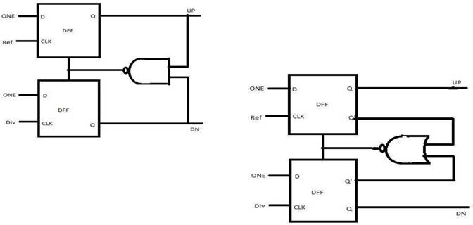
Fig.2 NAND Gate based PF
Fig.4 NOR Gate based PFD
The schematic of NOR Gate based PFD shown in Fig.5 which consisting of only 20 transistors.
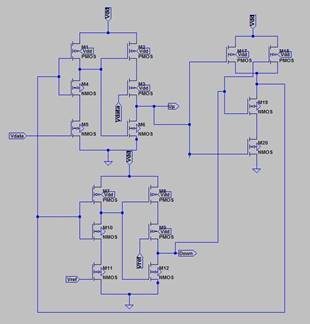
Fig.3 Schematic of NAND Gate based PFD
B.NOR Gate Based PFD
PFD using NOR gate is shown in figure.4. The circuit consists of two resettable, edge triggered
D flip flops with their D inputs tied to logic 1 and a NOR Gate in the reset path. The Ref and Div serve as clocks of the flip flops.
The UPb and DNb signals are given as input to the NOR gate. Suppose the rising edge of Ref leads that of
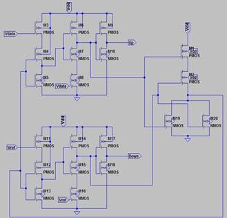
Fig.5 Schematic of NOR Gate based PF
C.AND Gate Based PFD
Fig.6 shows the PFD using AND gate. The circuit consists of two edge triggered D flip flops DFF which is resettable, with their D inputs tied to logic 1 and a AND Gate in the reset path. The Ref and Div serve as clocks of the flip flops. Suppose the rising edge of Ref leads that of Div, then UP goes to logic high. UP keeps high until a low to high transition occurs on Div. Because UP and DN, are AND, so Reset goes to logic high and resets the PFD into the initial state.
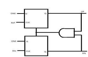
Fig.6 AND Gate based PFD
The schematic of AND gate based PFD circuit consisting of only 22 transistors is shown in Fig.7
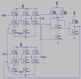
Fig.7 Schematic of AND Gate based PFD
III.SIMULATION RESULTS
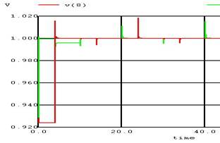
The PFD is a state machine with three states. When Ref leads Div, the UP output is asserted on the rising edge of Ref. The UP signal remains in this state until a low to high transition occurs on Div. At that time, the DN output is asserted causing both the flip flops to reset through the asynchronous reset signal. There is a small pulse on the DN output, whose duration is equal to the delay through the logic gates and the reset delay. The pulse width of the up pulse is equal to the phase error between the two signals.Here, Ref signal is equal to the Data Signal and Div signal is equal to the Clock signal.
B.NAND Gate PFD Simulation
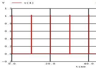
Input for same phase
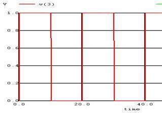
Output when both input clocks are in same phase


Output when both inputs are in d ifferent phase
B.AND Gate PFD Simulation
Output when both input clocks are in same phase
Output when both inputs are in d ifferent phase

IV. PERFORMANCE COMPARISON
Table I represents various parameters for the different PFDs when they are designed on NG Spice. It is seen that NAND based PFD has the minimum power consumption and occupy less area compared to the other two. They all have the same range of operating frequency. Dead Zone problem is also negligible for the NAND Based PFD.
Table I: Comparison between different PFD
|
Parameters |
AND |
NOR Based |
NAND Based PFD |
|
Based |
PFD |
||
|
PFD |
|||
|
Operating |
50 MHz |
50 MHz |
50MHz |
|
Frequency |
|||
|
Delay |
High |
Higher |
Low |
|
Power |
High |
Higher |
Low |
|
Consumption |
V. CONCLUSIONS
Minimization of power consumption is essential for high performance VLSI systems. This project compares the performance of Phase Frequency Detectors by different Logic Gates .As can be seen from the simulation results AND based PFD consumes maximum amount of power among all the PFDs and has highest delay. NOR based PFD consumes more area and power compared to the NAND based PFD.Therefore, in order to have low power consumption and smaller area we use NAND based PFD.