Home > mini projects > Generation of PWM using 555 timer IC
Generation of PWM using 555 timer IC
Abstract -PWM (Pulse Width Modulation) is one of the modulation techniques in which the width of the carrier wave varies with the amplitude of the message signal. In this technique the pulse is used as a carrier signal and the message signal can be any analog signal. Hence as the width is changing it can be used to control the power given to the devices. Thus the major application of PWM is to control the power given to the electrical appliances like motors.
This project presents one of the techniques of generation of Pulse Width Modulation using IC 555. IC 555 is a general purpose integrated circuit which is used in many applications as a function generator, timers, op-amps.
INTRODUCTION:
The PWM is also called as PDM (Pulse Duration Modulation) as the width or the duration of the pulse is varying. The leading edge of thepulse is fixed whereas the trailing edge is movable. In this document the PWM is implemented using 555 timer IC using ngspice.
WORKING OF THE CIRCUIT:
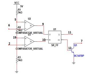
The circuit shown below in figure takes Sine wave of 200Hz frequency as message signal input and produces a PWM output. 555 timer is used in monostable vibrator mode. In this circuit, we gave the Sine wave as the control signal of the 555timer. The carrier pulse signal is used to trigger the output of the 555 timer. The duty cycle of the output depends on threshold level which is in turn dependent on control signal i.e message signal. In this way the output signal width varies with the amplitude of the input message signal which is PWM signal.
IMPLEMENTATION OF CIRCUIT:
The circuit is implemented using different softwares.
NGSPICE:
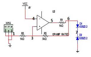
IC 555 is not available as an inbuilt model in ngspice. So for the generation of PWM using IC 555, this IC has to be modelled in the ngspice using comparators, resistors and SR flipflop.
For the creation of comparator we require an operational amplifier which is made of resistors, capacitor and dependent sources.
For the creation of SR flipflop we used several basic gates like inverter, two input nand gate, three input nand gate which are again modelled using subckt command of NGSPICE.
In the circuit the output of the comparator should be given to SR flipflop which takes either 0V or 5V, whereas the output of the comparator is ranging from -5V to +5V. So to make the output toggle between 0V and 5V we introduced an 'and' gate whose one input is given to Vcc and the other input is the comparator output.
The output of the and gate is used as the new output of the comparator.
MULTISIM:
It is a simulation tool used for the simulation of analog and digital circuits. IC 555 is available inbuilt in the multisim. The circuit is implemented using the circuit diagram shown below. The input message signal is given as a sine wave of 200 Hz and the input carrier signal is a pulse signal of 2kHz frequency. The output and the input message signals are observed in the inbuilt CRO in the multisim.
CIRCUIT LAB:
Circuit Lab is an online simulator which is similar to Multisim. The results of the simulation of the circuit are observed in the Circuit lab. These simulations helps us to debug the circuit and helps in writing the netlist of the circuit in NGSPICE.
ADVANTAGES:
PWM is somewhat similar to frequency modulation. Its advantages are:
Interference of noise is less or minimum.
System is moderate in complexity to implement.
It has moderate power efficiency among all three types that is PAM, PWM, PPM
It supports higher power handling capability.
DISADVANTAGES:
Even though PWM has a lot of advantages, it has the following drawbacks.
Instantaneous power of transmitter varies.
The system requires semiconductor devices with low turn
ON and turn- OFF times. Thus they are very expensive.
High switching losses due to higher PWM frequency.
APPLICATIONS:
Pulse width modulation has many applications which include highly sophisticates electrical circuits.
It also finds its applications in field of Robotics for the control of speeds of motors.
In small applications, it can be used to control the brightness of the LEDs by changing the duty cycle of the pulse carrier. It is also used in controlling the angle of the servo motors which are used in robotics.
ABBREVIATIONS AND ACRONYMS:
PWM-Pulse Width Modulation PAM-Pulse Amplitude Modulation PPM-Pulse Position Modulation CRO-Cathode Ray Oscilloscope PDM-Pulse Duration Modulation
CIRCUIT DIAGRAM:
NETLIST:
pwm
.include timer.cir
R1 4 6 6.8K
R2 1 5 10K
R3 3 0 25K
C1 6 0 0.1u
V2 2 0 pulse(0 5 1n 1n 1n 0.5m 1m)
V1 1 0 sin(0 2 200 0 0 0)
vcc 4 0 5V
x51 2 5 6 6 3 tim
.control
tran .01m 2m
run
plot v(1)
.endc
.end
IC 555 CIRCUIT DIAGRAM:
IC 555 SUBCKT NETLIST:
ic555
.subckt tim 2 5 6 7 3
.include comp.cir
.include sr.cir
.model bjt1 npn
R1 8 5 5k
R2 5 19 5k
R3 19 1 5k
Vcc 8 0 5V
V1 1 0 0V
xsr1 10 9 3 12 sr1
xc1 6 5 9 comp1
xc2 19 2 10 comp1
Q1 7 12 0 bjt1
.ends
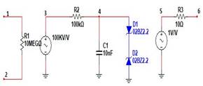
COMPARATOR SUB CIRCUIT:
NETLIST OF COMPARATOR SUBCKT:
COMPARATOR
.subckt comp1 1 4 11
.include opamp2.cir
.include nandtwo.cir
.include inv.cir
.model DZ1 D(Is=0.05u Rs=0.1 Bv=4.3 Ibv=0.05u)
.model DZ2 D(Is=0.05u Rs=0.1 Bv=4.3 Ibv=0.05u)
R1 2 3 1K
R2 3 6 5K
XOP2 3 4 5 OPAMP1
RLIM 5 6 1000
D1 7 6 DZ1
D2 7 0 DZ2
VREF 4 0 0V
v3 8 0 5V
xn1 6 8 10 nan2
xi1 10 11 not
VNOISE 2 1 SIN(0V 0VPEAK 2.5KHZ)
.ends
OPAMP SUB CIRCUIT:
NETLIST OF OPAMP SUBCKT:
opamp
.subckt opamp1 1 2 6
.model dz0 d(is=0.05u rs=0.1 bv=15 ibv=0.05u)
rin 1 2 10meg
egain 3 0 1 2 100k
|
rp1 |
3 4 100k |
|
cp1 |
4 0 0.0159uf |
ebuffer 5 0 4 0 1
rout 5 6 10
|
d1 4 |
7 |
dz0 |
|
d2 0 |
7 |
dz0 |
|
.ends |
||
OTHER SMALL SUB CIRCUITS:
INVERTER:
*inverter*
.model mosn nmos
.model mosp pmos
.subckt not 1 2
m1 2 1 0 0 mosn
m2 2 1 3 3 mosp
vdd 3 0 dc 5
.ends
TWO INPUT NAND GATE:
*nand2 ip gate*
.model mosn nmos
.model mosp pmos
.subckt nan2 1 2 4
m1 3 2 0 0 mosn
m2 4 1 3 3 mosn
m3 4 1 5 5 mosp
m4 4 2 5 5 mosp
vdd 5 0 dc 5
.ends
THREE INPUT NAND GATE:
*nand3ip gate*
.model mosn nmos
.model mosp pmos
.subckt nan3 1 2 3 6
m1 4 3 0 0 mosn
m2 5 2 4 4 mosn
m3 6 1 5 5 mosn
m4 6 1 7 7 mosp
m5 6 2 7 7 mosp
m6 6 3 7 7 mosp
vdd 7 0 dc 5
.ends
SR FLIPFLOP:
*SR*
.SUBCKT sr1 1 2 5 6
.include inv.cir
.include nandtwo.cir
.include nandthree.cir
x1 1 3 not
x2 2 4 not
x3 3 6 5 nan2
x4 4 5 6 nan2
.ends
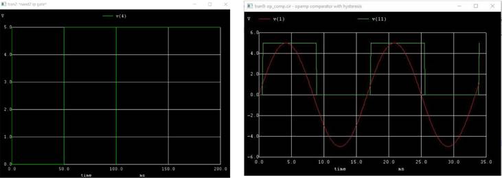
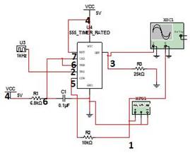
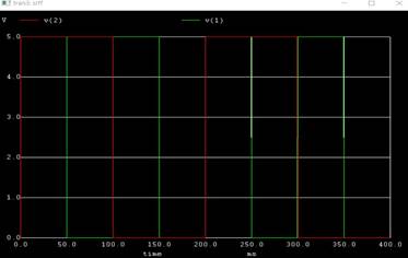
RESULTS:
PWM SIMULATION RESULTS:
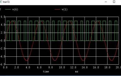
Green- PWM output
Red- sine signal as Input Message
MULTISIM SIMULATION OUTPUT:
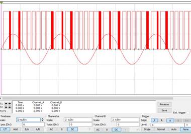
Channel1-- PWM output
Channel2-- sine signal as Input Message
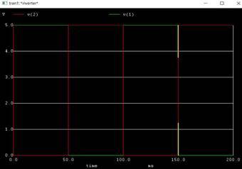
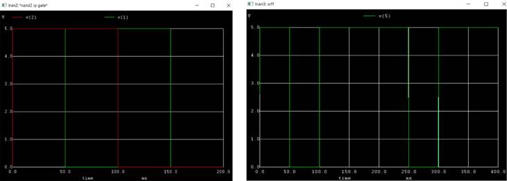
SUBCIRCUIT SIMULATIONS:
INVERTER:
SR FLIPFLOP:
INPUTS:
|
TWO INPUT NAND GATE: |
OUTPUT AT Q: |
|
INPUTS: |
OUTPUT: COMPARATOR: