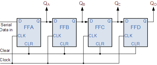
The operation of SIPO is as follows. Lets assume that all the flip-flops ( FFA to FFD ) have just been RESET ( CLEAR input ) and that all the outputs QA to QD are at logic level “0” ie, no parallel data output.
If a logic “1” is connected to the DATA input pin of FFA then on the first clock pulse the output of FFA and therefore the resulting QA will be set HIGH to logic “1” with all the other outputs still remaining LOW at logic “0”. Assume now that the DATA input pin of FFA has returned LOW again to logic “0” giving us one data pulse or 0-1-0.
The second clock pulse will change the output of FFA to logic “0” and the output of FFB and QB HIGH to logic “1” as its input D has the logic “1” level on it from QA. The logic “1” has now moved or been “shifted” one place along the register to the right as it is now at QA.
When the third clock pulse arrives this logic “1” value moves to the output of FFC ( QC ) and so on until the arrival of the fifth clock pulse which sets all the outputs QA to QD back again to logic level “0” because the input to FFA has remained constant at logic level “0”.
The effect of each clock pulse is to shift the data contents of each stage one place to the right, and this is shown in the following table until the complete data value of 0-0-0-1 is stored in the register. This data value can now be read directly from the outputs of QA to QD.
Then the data has been converted from a serial data input signal to a parallel data output. The truth table and following waveforms show the propagation of the logic “1” through the register from left to right as follows.