IC Testing
Testability is the property of a circuit that makes it easy to test. The testability is highly dependent on testing. Consider the example in which design engineer considers complexity of test vector generation to test the circuit. Now the test engineer, testability is compatibility of design with test equipment. Quality engineers relates testability to fault coverage. By increasing the testability of a circuit, some function of the costs is reduced. For example, scan designs lower the cost of test generation and increase the number of I/O pins, area, and test time. Testability is a design characteristic due to which various costs associated with testing and the cost-effective development of the tests to determine the status.
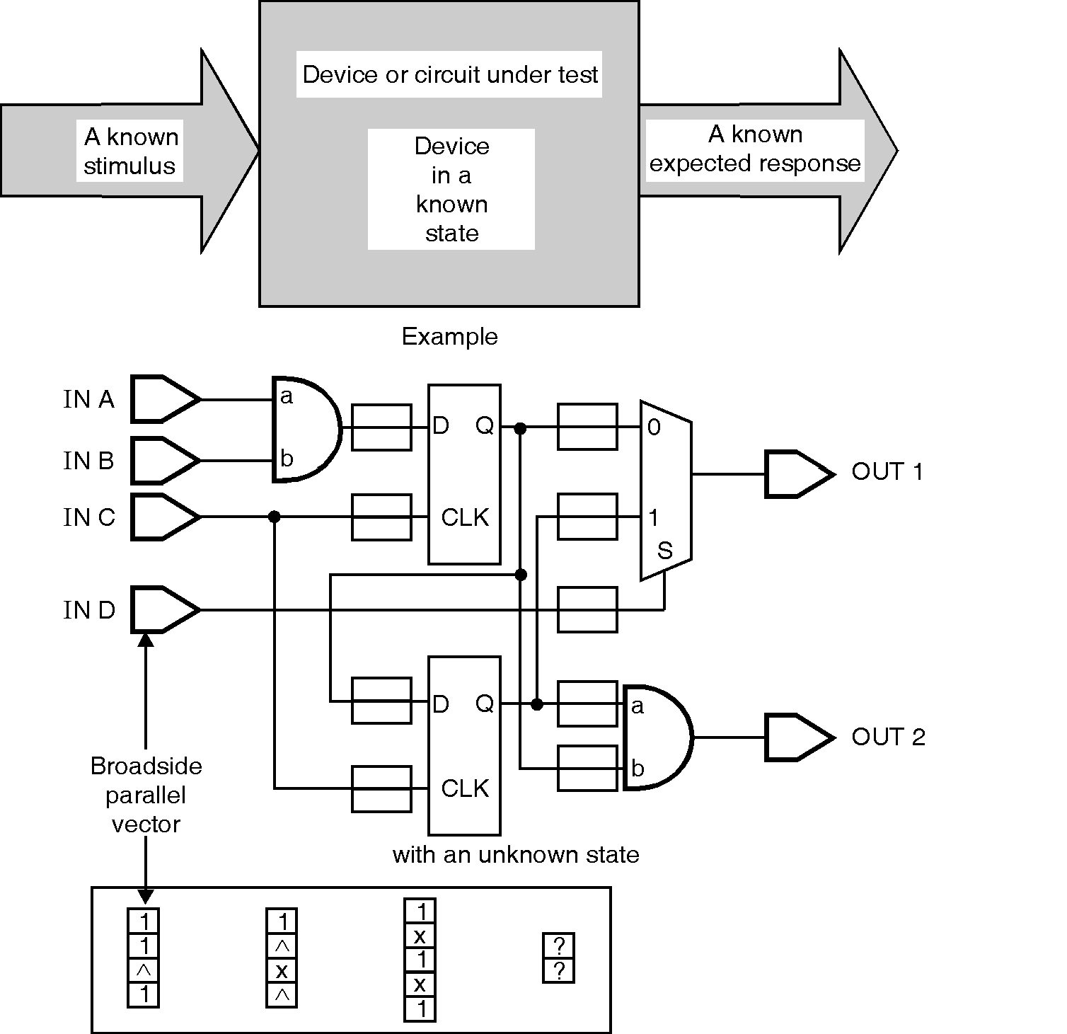
What is testing ?
The definition of testing is a simple concept and it applies equally to chips, boards and systems. Testing is possible when a known input is applied to a unit in a known state, and a known response can be evaluated. In general, figure below shows, the known response from a circuit is compared to an expected response.
Testing can be accomplished on any circuitry from transistors, gates, macrocells, cores, chips, boards, and systems. Design for Testability is adding logic to enhance the testability of a design. Design for Testability is defined by adding features to enhance ability to achieve quality metrics for,
- To easily generate vectors
- To reduce the time in vector generation
- To reduce the cost of vectors.
Advantages and Disadvantages of DFT :
- DFT adds complication to the design flow.
- DFT increase power, area, timing and package pins.
- DFT adds risk to the design schedule.
- DFT increases ability to measure the quality.
- DFT generate the necessary vectors easily.
- Reduces tester complexity
- Reduces tester time
- Reduces tester requirements