Scan Path Testing :
A scan path can be created by the logic designers who are designing the circuit, or it can be created by software during the synthesis process. when scan is designed into the ICs, it is designed for optimal testing of the IC, without efforts. During test the flip-flops are configured for serial shift mode. In serial shift mode, logic values are loaded by serially shifting in the desired values. Figure below shows a simple technique for creating the scan path which consists of placing a multiplexer just ahead of each flip-flop. One input to the 2:1 multiplexer is driven by normal operational while the other input with one exception is driven by the output of another flip-flop. The multiplexer control line, connected to a primary input pin in mode control. Mode control gives the parallel load for normal operation and selects serial shift. The scan path can be tested by shifting a special pattern through the scan path before even beginning to address stuck-at faults in the combinational logic.
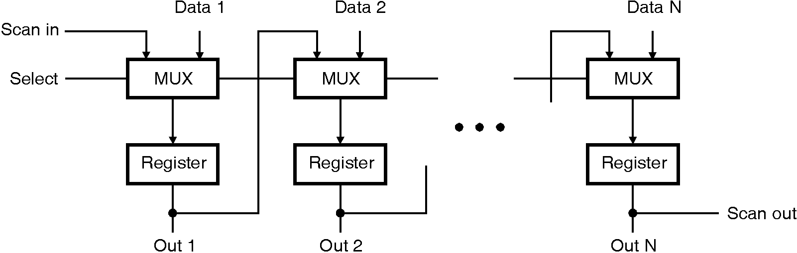
During the generation of test patterns, the automatic test pattern generation considers the flip-flops as I/O pins. When circuit with scan path is operated in the normal mode, the mode control, or test control, is set for parallel load. when the device is to be tested, the mode control alternates between parallel load and serial shift. During the operation that data are compared to expected data to determine whether the faults are present in the circuit.
Scan path advantages and Disadvantages:
- Test vectors can be generated by automatic test pattern generation programs.
- Observability/Controllability problems do not have to be considered during the design phase.
- Testers do not need to have complex test vector generation capabilities for all pins of the chip.
- Additional multiplexers must be included in the circuit.
- Additional multiplexers added in signal path.