Home > Analog CMOS Design > MOSFET Amplifiers > Push Pull Inverter
Push Pull Inverter :
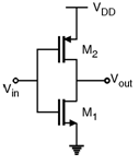
Figure below shows the circuit diagram of the push pull inverter circuit. In this configuration the gates of the two transistors are connected together and the input signal is applied at this combination. Also, the drains of the both PMOS and NMOS transistors are shorted together and the output response is measured at this combination.
The small signal equivalent circuit of this configuration is shown in Figure below
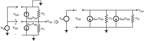
By applying KCL,
We get, gm1 VGS + + gm2 VGS + = 0
gm1 Vin + + gm2 Vin + = 0
(gm1 + gm2) Vin = - Vout
\ = -
\ An = -