Home > Digital CMOS Design > Non Ideal Effects > Subthreshold Conduction
Subthreshold-Conduction | Digital-CMOS-Design
Subthreshold Conduction :
In order to address the subthreshold conduction phenomenon let us plot the
IDS-VGS characteristics shown in Figure below.
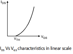
A closer inspection of the IDS-VGS curve shows that the current does not drop abruptly to '0' at VGS = VTH. It indicates that the MOS transistor is partially conducting for voltages below the threshold voltage. This effect is called as subthreshold or weak inversion conduction. To study subthreshold conduction effect in more detail let us redraw the curve of on logarithmic scale as shown in Figure below.
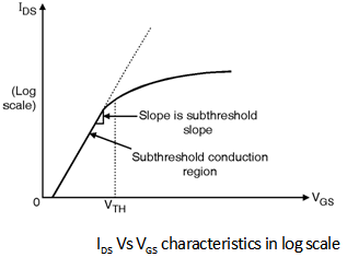
From the IDS-VGS curve in log scale it is clear that current does not drop to zero immediately for VGS < VTH but actually decays in an exponential fashion.
Thus even VGS < VTH IDS is finite but it exhibits exponential dependence on VGS for smaller values of VDS roughly in the range of 200 mV.
The subthreshold conduction effect can be formulated as :
IDS = I0 exp VGSn KTq
Where n > 1 is a non ideality factor.
• In digital circuit designs the presence of subthreshold current is not desirable because it deviates the transistor from its ideal switch like behaviour which require that current should drop as fast as possible once the gate to source voltage falls below VTH.
• The subthreshold conduction behaviour is represented subthreshold slope factor (S) which indicates the change in VGS for one decaded change in drain current. The unit of S is mV/decade.
• From the above Equation we can show that,
S = n KTq ln (10)