The SR (Set-Reset) flip-flop is one of the simplest sequential circuits and consists of two gates connected as shown in figure. Notice that the output of each gate is connected to one of the inputs of the other gate, giving a form of positive feedback or ‘cross-coupling’. The circuit has two active low inputs marked S and R, ‘NOT’ being indicated by the bar above the letter, as well as two outputs, Q and Q. Table shows what happens to the Q and Q outputs when a logic 0 is applied to either the S or R inputs.
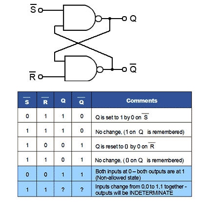
The SR Flip-flop Truth Table
- Q output is set to logic 1 by applying logic 0 to the S input.
- Returning the S input to logic 1 has no effect. The 0 pulse (high-low-high) has been ‘remembered’ by the Q.
- Q is reset to 0 by logic 0 applied to the R input.
- As R returns to logic 1 the 0 on Q is ‘remembered’ by Q.
Problems with the SR Flip-flop
In the table Q is the inverse of Q. However, in row 5 both inputs are 0, which makes both Q and Q = 1, and as they are no longer opposite logic states, although this state is possible, in practical circuits it is ‘not allowed’. In row 6 both inputs are at logic 1 and the outputs are shown as ‘indeterminate’, this means that although Q and Q will be at opposite logic states it is not certain whether Q will be 1 or 0, Notice however that in the absence of any input pulses, both inputs are normally at logic 1. This is normally OK, as the outputs will be at the state remembered from the last input pulse. The indeterminate or uncertain logic state only occurs if the inputs change from 0, 0 to 1, 1 together. This should be avoided in normal operation, but is likely to happen when power is first applied. This could lead to uncertain results, but the flip-flop will work normally once an input pulse is applied to either input. The SR Flip-flop is therefore, a simple 1-bit memory. If the S input is taken to logic 0 then back to logic 1, any further logic 0 pulses at S will have no effect on the output.
The Clocked SR Flip-flop
Figure below shows a useful variation on the basic SR flip-flop, the clocked SR flip-flop. By adding two extra NAND gates, the timing of the output changeover after a change of logic states at S and R can be controlled by applying a logic 1 pulse to the clock (CK) input. Note that the inputs are now labeled S and R indicating that the inputs are now ‘high activated’. This is because the two extra NAND gates are disabled while the CK input is low, therefore the outputs are completely isolated from the inputs and so retain any previous logic state, but when the CK input is high (during a clock pulse) the input NAND gates act as inverters.
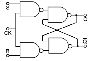
The main advantage of the CK input is that the output of this flip-flop can now be synchronized with many other circuits or devices that share the same clock. This arrangement could be used for a basic memory location by, for example, applying different logic states to a range of 8 flip-flops, and then applying a clock pulse to CK to cause the circuit to store a byte of data.