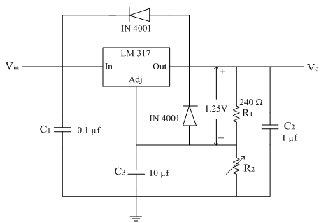
The LM 317 is an example of a three terminal positive voltage regulator with adjustable output voltage. The standard configuration of this regulator is shown below.

The capacitors are used for decoupling and don't affect the dc operations. There is one input, one output and one adjustable terminal. The external fixed resistor R1 and variable resistor R2 provide the output voltage adjustment.
The output voltage can be varied from 1.2V to 37V depending upon the resistor values. The LM 317 can provide up to 1.5A current to a load.
The LM 317 is operated as a floating regulator because the adjustment terminal is not connected to ground; but floats to whatever voltage is across R2. This allows output to be much higher than that of a fixed voltage regulator.
Operation:
As shown in figure below, a constant 1.25V reference voltage (Vref) is maintained by the regulator between the output terminal and the adjustment terminal.
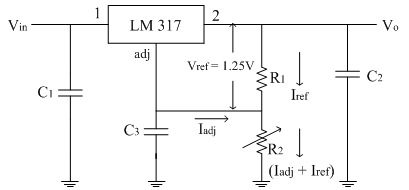
This constant reference voltage produces a constant reference current called Iref through R1 regardless the value of R2. The current through adjustment terminal and Iref flows through R2.
∴Iref=Vref/R1 =1.25/R_1
Also there is a very small constant current at the adjustment terminal called Iadj which flows through R2. It is approximately of 50µA.
The output voltage is given as
Vo=V(R1 )+V(R2 )
∴Vo=Iref R1+[Iadj+Iref ] R2
∴Vo=Iref R1+Iadj R2+Iref R2
∴Vo=Iref [R1+R2 ]+Iadj R2
∴Vo=Vref/R1 [R1+R2 ]+Iadj R2
∴Vo=Vref [(R1+R2)/R1 ]+Iadj R2
∴Vo=Vref [1+R2/R1 ]+Iadj R2
Thus the output voltage is proportional to resistance R2. The output voltage can be made variable by making resistance R2 variable and keeping R1 fixed.
Thus by varying R2, output voltage can be adjusted. Typically Iadj is very small (50µA to 100µA) so generally neglected.
∴Vo=1.25[1+R2/R1 ]
Functional block diagram of LM 317:
As seen in previous section, the output voltage is a function of R1 and R2. Keeping R1 fixed and R2 variable, output voltage can be adjusted. The resistor R1 is generally selected as 240Ω.
∴Vo=1.25[1+R2/R1 ]
If LM 317 is located far from the power supply filter, then the capacitors C1 and C2 are required. The input capacitor C1 is generally 0.1µf disc or 1µf tantalum while the output capacitor C2 is in the range of 1µf to 1000µf.
To get high ripple rejection, the capacitor C3 is used. To avoid the discharging of the capacitor through the low current points into the regulator, the protecting diodes are used (The diodes are required if output is higher than 25V).
∴Vo=1.25[1+R2/R1 ]