Home > Digital CMOS Design > CMOS Layout Design > CMOS Design Flow
CMOS-Design-Flow
CMOS Design Flow : Figure below shows the CMOS IC design flow, it consists of defining circuit inputs and outputs also called as specifications of the circuit. Once the detailed list of inputs and outputs is developed from this the design calculations are performed and the circuit schematic for the intended integrated circuit is designed. This developed schematic is then drawn in CAD (Computer Aided Design) tools e.g. Tanner. Once the schematic entry is finished then the circuit simulations are carried out and the obtained simulation results are checked with the intended specifications this step is called as pre-layout simulation. After checking post layout simulation results, the next step is the fabrication of the prototype board. Once the fabricated board comes the testing of the protype is carried out and the initial specifications are checked, if these results are not matched with the intended specifications then there are two possibilities of error that may be either because of fabrication or initial specification problem. If the prototype board passed all the tests then it is given for mass production. This flow is used for custom IC design. A custom designed IC is also called as ASIC (Application Specific Integrated Circuit). Other noncustom methods of designing chips includes FPGA (Field Programmable Gate Arrays) and standard cell libraries. The FPGA and standard cell approach is used when low volume and quick design turnaround are important. Most of the chips that are mass produced such as microprocessors and memories are manufactured using the custom design approach shown in Figure.
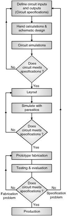
Fig-CMOS-Design-Flow