A circuit in which output voltage waveform is the time integral of the input voltage waveform is called integrator or integrating amplifier.
The following circuit shows a basic/ideal integrator using op-amp,

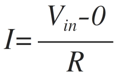
The non-inverting input terminal is at ground potential and hence, the inverting terminal is appearing to be at ground potential. The current 'I' through the resistance R is given as,
The input current to op-amp is zero so same current 'I' flows through the capacitor 'C' in feedback path also and is given as,

Comparing the above two equations for current 'I' we get,
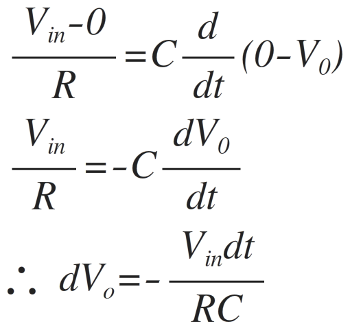
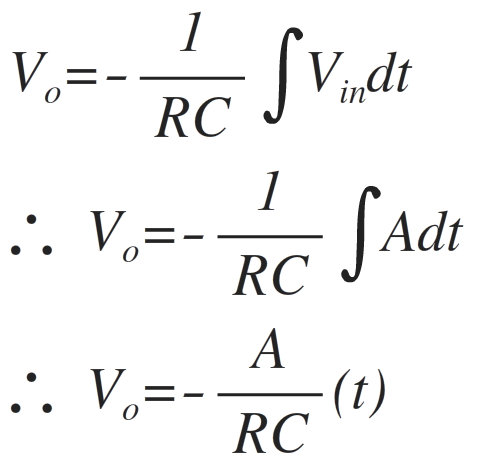
Integrating both the sides, we get,

where – 1/RC=≫Gain / scale factor of an integrator.
Thus output voltage is nothing but time integration of the input signal and hence acting as an integrator.
Now let us see what is the response of the integrator to the different types of input signals.
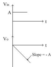
1) Vin = Step signal
The step signal is defined as follows
Vin (t)=A for t>0
Let the product RC = 1.
The output voltage is given as,
Thus for the positive step signal, output is a negative ramp signal with slope(-A/RC). At a particular't', integrator goes into negative saturation, so continuous dc signal is avoided for integrator. The input and output waveform is shown below.
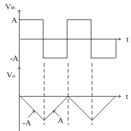
2) Vin = Square Wave
The square wave is nothing but combination of positive and negative step signals. As seen in first case, the output of step signal is a ramp signal. For positive step signal, a negative ramp and for negative step signal, a positive ramp is obtained because it is inverting integrator.
Thus for a square wave input, the output obtained is a triangular waveform as shown in figure below.
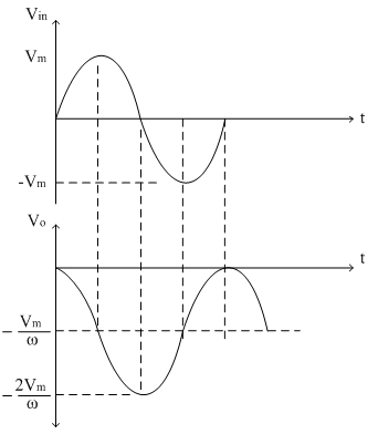
3)Vin = Sine Wave
Let Vin=Vm sinωt
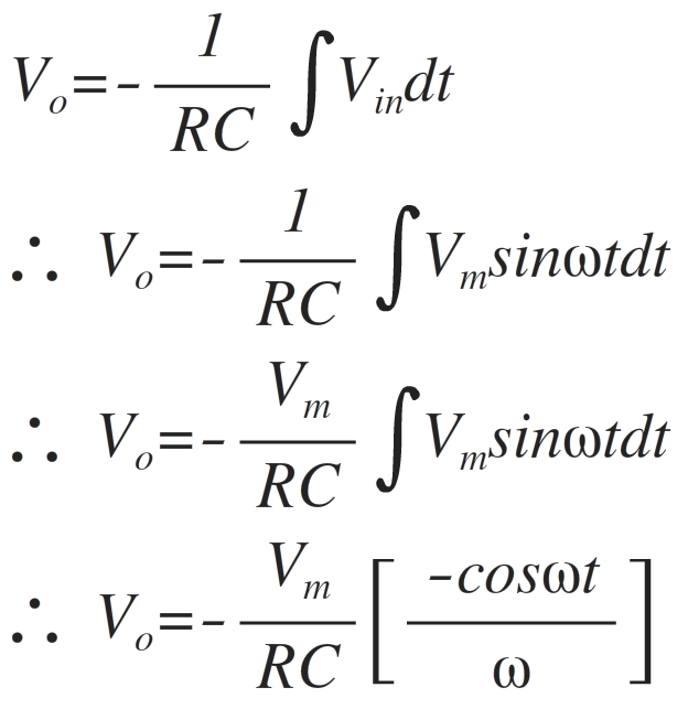
Thus the cosine wave is obtained as follows.
Frequency response of ideal integrator:
The ideal integrator is shown below using op-amp.
The gain of this amplifier is given as,
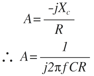
The magnitude of gain A is,
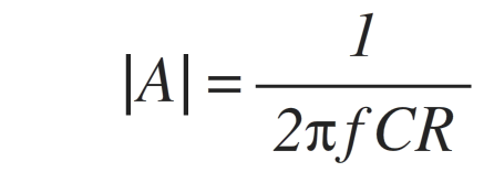
Thus the gain A is inversely proportional to frequency f.
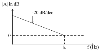
At low frequency, the gain is very high. As frequency increases, gain starts decreasing linearly at the rate of -20dB/decade.
For dc input (f = 0) the gain is almost infinite. This is because the reactance of capacitance (Xc) becomes very high for low frequencies. Thus it acts as an open circuit and op-amp goes into open loop configuration. In open loop configuration gain of op-amp is almost infinite. As frequency increases gain starts dropping at the rate of -20dB/decade. Thus the response is similar to Low Pass Filter.
Let, the frequency f = fb is frequency at which gain of the op-amp becomes unity (=1) i.e. o dB.
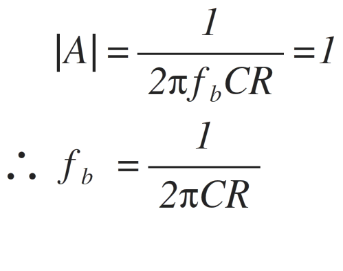
Thus gain drops to 0 dB at a frequency f=fb, from its very high value at low frequencies. The frequency response of ideal integrator is shown below.
Drawbacks in ideal integrator:
1. Bandwidth is very small and used for only small range of input frequencies.
2. For dc input (f = 0), reactance of capacitance, Xc is infinite. Because of this op-amp goes into open loop configuration.In open loop configuration the gain is infinite and hence the small input offset voltages are also amplified and appears at output as error. This is referred as false triggering and must be avoided.
Due to all such limitations, an ideal integrator needs to be modified. Some additional components are used along with ideal integrator circuit to reduce the effect of an error voltage in practice. This modified integrator is referred as practical integrator.