Home > Analog CMOS Design > MOSFET Parasitics > Parasitic capacitance Models
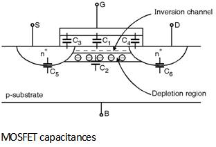
In integrated circuits the capacitances associated with the devices are taken into account to understand the behaviour of the circuits. For this purpose a model of capacitances is needed. The various capacitances associated with the MOSFET are shown in Figure below. The various capacitance involved are,
C1 Þ gate Oxide capacitance
C2 Þ Depletion capacitance
C3 Þ Overlap Capacitance between gate poly and the source
C4 Þ Overlap Capacitance between gate poly and the drain
C5 Þ Junction capacitance between source and the substrate
C6 Þ Junction capacitance between drain and the substrate
The gate capacitance (Cg) is decomposed into two elements each with different behaviour, one part of Cg contributes to the channel charge and another part is due to the MOS structure.
The channel charge capacitance is derived from the gate to channel capacitance CGC which consists of, 1) gate to source (CGCS), 2) gate to drain (CGCD), and 3) gate to Body (C GCB) capacitances. These capacitances are depend upon the operation region and terminal voltages. When the transistor is in the cut-off region no channel exists and CGC appears between gate and body.
In the linear region an inversion layer is formed which acts as a conductor between source and drain. Hence CGCB = 0 as the body electrode is shielded from the gate by the channel and by using the symmetry the total capacitance CGC is distributed evenly between source and drain.
In the saturation mode the channel is pinched off hence the capacitance between gate and drain is CGCD = 0 as well as the capacitance between gate and body i.e. CGCB = 0 therefore the total capacitance CGC is represented by the gate to source capacitance CGCS.
The actual value of the total Gate to channel capacitance (CGC) its distribution over three components (CGCB, CGCS and CGCD) is given as below :
For VGS = 0 the transistor is OFF no channel is present and the total capacitance appears between gate and body which is given as :
CGC = Cox × W × L
When we increase VGS a depletion region forms under the gate this appears as an increase in the thickness of the gate dielectric which results in a reduction in capacitance. Which was shown in C-V characteristics in Fig. 8.6.4 once the transistor turns ON (VGS = VTH) a channel is formed and CGCB drops to '0' with VDS = 0 the devices operates in the linear mode and the total capacitance is divided equally between source and drain which is given as :
CGCS = CGCD =
Once the transistor is ON the distribution of its gate capacitance depends upon the degree of saturation measured by the ratio .
In the saturation mode CGCD gradually drops to '0' for increasing the levels of saturation while CGCS increases. Hence the total gate to channel capacitance is represented by CGCS which is given as :
CGCS = Cox × W × L
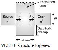
Consider the structure of MOS transistor shown in Figure below. Ideally the source and drain diffusion should end right at the edge of the gate oxide.
But in reality both source and drain tend to extend some what below the oxide by an amount LD called as lateral diffusion. Hence the effective channel length of the transistor becomes shorter than the drawn length Ldrawn by a factor 2 LD. This gives rise to a parasitic capacitance between gate and source as well as gate and drain this type of capacitance is called as the overlap capacitance. This capacitance is given as :
Cgso = Cox × LD × W and Cgdo = Cox × LD × W
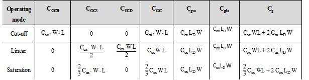
The average distribution of all the gate capacitance in cut-off, linear and saturation region of operation is given in Table below.
The diffusion capacitance also called as junction capacitance is contributed by the reverse biased source-body and drain-body pn junctions. This type of junction capacitance is non linear and decreases when the reverse bias is increased.
The components of diffusion capacitance at source or drain region are shown
in
Figure below. The diffusion capacitance also includes the capacitances due
to bottom plate junction and side wall junctions.
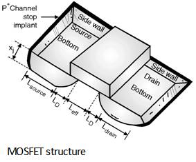
The bottom plate junction is formed between source and the substrate. This capacitance is given by,
Cbottom = Cj W × Lsource
Where Cj is the junction capacitance per unit area.
Further, the side wall junction is formed by source and channel stop implant This capacitance is expressed as,
Csw = Cjsw ´ (W + 2 Lsource)
Thus, Total diffusion capacitance for source is expressed as,
Cdiff = Cbottom + Csw = Cj ´ Area + Cjsw ´ Perimeter
= Cj Lsource W + Cjsw (W + 2 L source)
Further, the total diffusion capacitance for drain side is expressed as, :
Cdiff = Cj Ldrain W + Cjsw (W + 2 Ldrain)
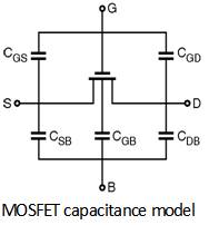
Capacitance Device Model of MOSFET :
All the contributions of capacitances can be combined in a single model for the MOS transistor as shown in Figure below.The equation which relates all the capacitances is given as :
![]() CGS = CGCS + GGSO ;
CGS = CGCS + GGSO ;
CGD = CGCD + CGDO ;
CGB = CGCB
CSB = CS diff
CDB = CD diff
Thus for designing high performance and low energy circuits to this model is strongly required.