Home > mini projects > ANALOG TRNSMITTER AND RECEIVER
Abstract-Design of Analog Transmitter and Receiver using MOSFETS for optimization of power dissipated and maximization of bandwidth. Design of transmitter circuit according to current levels at the output and design of receiver using common gate amplifier cascade.
I. I NTRODUCTION
Communication means exchange of information through signals. It can be of two types 1.Analog Communication 2.Digital Communication. Analog communication means the signals which are used are continuous in time domain and amplitude domain. Digital communication means the signals which are used are discrete in time domain and amplitude domain. For communication we need transmitter and receiver. Transmitter means a set of equipment used to transmit messages. Receiver means a set of equipment used to receive the transmitted signals. There are many factors to consider while communication they are: consider 1.Bandwidth 2.Speed of transmission 3.Noise immunity 4.Power dissipation 5.Signal attenuation. Hence our objective is to design an analog transmitter and receiver circuit with optimization in power dissipation and maximization of bandwidth. We design the transmitter and Receiver using Metal Oxide Semiconductor Field Effect Transistors(MOSFETS).We used MOSFETS to design the current mirror circuit and the differential amplifier circuit on the transmitter side and common gate amplifier on the receiver side. Clear cut design of transmitter and receiver is presented below.
II. DESIGN OF TRANSMITTER
We give pulse as input signal and get dc current by using a current mirror. A current mirror is a circuit designed to copy a current through one active device by controlling the current in another active device of a circuit, keeping the output current constant regardless of loading. The current being 'copied' can be, and sometimes is, a varying signal current. Conceptually, an ideal current mirror is simply an ideal inverting current amplifier that reverses the current direction as well or it is a current-controlled current source. The current mirror is used to provide bias currents and active loads to circuits. It can also be used to model a more realistic current source (since ideal current sources don't exist).
This setup only allows the current when gate voltage is very high. Here the voltage pulses we are giving as input are transmitted as current pulses through channel. Clock is fed through and an alternative path is provided by another pair of MOSFETS so that there is always current flowing in the current mirror branch. There pulse is given in inverted form as input. The resistor values and (W/L) values are chosen so that all the MOSFETs are in saturation region as well as for getting least rise time.
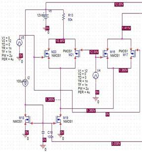
Fig1: circuit diagram of the transmitter
Here the pulse signal which is given as input is transmitted in the form of current pulses through the transmitter. The current mirror output is connected to the differential amplifier input. The differential amplifier is constructed using NMOS and PMOS. From the differential amplifiers output is the output of the transmitter. The output wave form of the transmitter is as follows
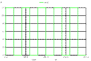
Fig2: Input pulse waveform
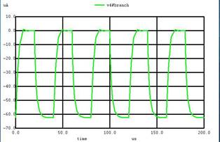
Fig3: Output of the transmitter
III. DESIGN OF THE RECEIVER
In the receiver circuit part we have to use a common gate amplifier so that it may act as a current to voltage amplifier. In electronics, a common gate amplifier is one of three basic single-stage field- effect transistor (FET) amplifier topologies, typically used as a current buffer or voltage amplifier. In this circuit the source terminal of the transistor serves as the input, the drain is the output and the gate is connected to ground, or
|
"common," hence |
its |
name. The |
analogous bipolar junction |
|
|
transistor circuit |
is |
the common-base |
amplifier. This |
|
|
configuration is |
used less |
often |
than the common |
|
source or source follower. It is useful in, for example, CMOS RF receivers, especially when operating near the frequency limitations of the FETs; it is desirable because of the ease of impedance matching and potentially has lower noise. Gray and Meyer provide a general reference for this circuit.
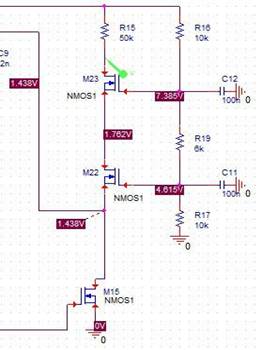
But the MOSFET connected to Rd should must have least W/L ratio to order to minimize the rise time (as W/L of a MOS increases the parasitic capacitances values also increases ).So to get higher gain and bandwidth we use cascade in which the upper MOS is having less W/L ratio where as the second one is with higher W/L ratio to get higher gain. But if we use feed which increases the bandwidth significantly will decrease the gain. That's why we preferred using cascade amplifier. The output waveforms are as follows. We get the output waveform as the pulse waveform which is input. There will be some distortion.
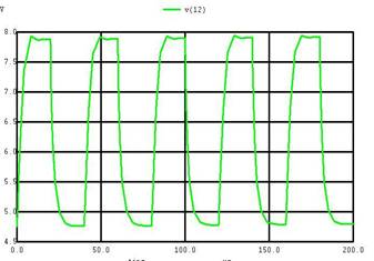
Fig3: Receiver output
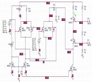
Fig 4:Complete circuit diagram
SIMULATION :
Circuit simulation is done using NGSPICE software and the code is as follows
ANALOG TRANSMITTER AND RECEIVER
.model mos1 nmos (vto=1.5)
.model mos2 pmos (vto=1.5)
v1 4 0 pulse(0 12 0 1n 1n 20u 40u)
v2 0 6 pulse(12 0 0 1n 1n 20u 40u)
v3 2 0 dc 12
v4 8 13 dc 0
i1 2 1 dc 100ua
c9 8 0 .2n
c10 1 0 100n
c11 9 0 100n
c12 11 0 100n
r12 7 8 500
r13 1 3 100k
r15 2 12 50k
r16 2 11 10k
r17 9 0 10k
r19 9 11 6k
m15 13 1 0 0 mos1 w=4 l=1
m16 7 6 5 5 mos1 w=4 l=1
m17 5 4 7 7 mos2 w=4 l=1
m18 1 1 0 0 mos1 w=4 l=1
m19 5 1 0 0 mos1 w=4 l=1
m20 3 4 5 5 mos1 w=4 l=1
m21 5 6 3 3 mos2 w=4 l=1
m22 10 9 13 13 mos1 w=12 l=1
m23 12 11 10 10 mos1 w=1 l=1
.tran 20u 200u
.control
run
display
set color0=white
set color1=black
set xbrushwidth=3
plot v(12)
plot v(4)
plot v4#branch
.endc
.end
IV. OPTIMISATION
Bandwidth depends on the input conductance high bandwidth means maximization of input conductance. Input conductance depends on the drain current and w/l ratio. Input conductance can be maximized using high drain current and small w/l ratio or small drain current and high w/l ratio. Our target is to minimize total power dissipation for that purpose we use small drain current and high w/l ratio. But high w/l ratio means high rise time. There will be more distortion in the output as compared to the input.
|
WIDTH(micro m) |
RISE TIME(seconds) |
|
|
1 |
1.69009E-06 |
|
|
2 |
1.23457E-06 |
|
|
3 |
1.10323E-06 |
|
|
4 |
1.04831E-06 |
|
|
5 |
1.03021E-06 |
|
|
5.15 |
1.03721E-06 |
|
|
5.2 |
1.02326E-06 |
|
|
5.25 |
1.02642E-06 |
|
|
5.5 |
1.02665E-06 |
Table 1: Variation of rise time with width keeping length constant
Therefore we observed that by using low drain current and high w/l ratio not too high but to a certain acceptable extent we can design an analog transmitter and receiver with minimum power dissipation and maximum bandwidth.