Home > Analog CMOS Design > MOSFET Amplifiers > Common Drain Amplifier
Common Drain Amplifier (Source Follower) :
Figure below shows the source follower circuit in which drain terminal of the device is common. In this circuit the drain terminal is directly connected to VDD.
In CS amplifier analysis we have seen that in order to achieve the high voltage gain the load impedance should be as high as possible. Therefore for low impedance load the buffer must be placed after the amplifier to drive the load with negligible loss of the signal level. The source follower thus worked as a buffer stage. The source follower is also called as the common drain amplifier.
In this circuit, the signal at the gate is sensed and drives the load at the source which allows the source potential to follow the gate voltage. The small signal equivalent circuit of the source follower is shown in Figure below.
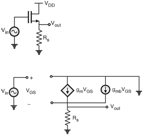
by analysing the circuit, the voltage gain is given by,
=
Form this equation it can be seen that, as gm increases the A v approaches to = 1.
Therefore eventually Av approaches to unity.
Further, the source follower exhibit a high input impedance and a moderate output impedance. The drawback of source follower are nonlinearity due to body effect and poor driving capability of the input signal.