Home > Digital CMOS Design > CMOS Inverter > Power Delay Product in CMOS
Power- Delay Product in CMOS
Power- Delay Product in CMOS :
The power-delay product (PDP) is defined as a product of power dissipation and the propagation delay. Figure below shows the shows the PDP input signal waveform.
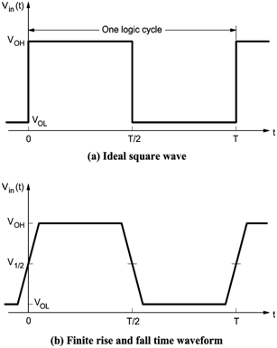
Fig1-Power-Delay-Product-in-CMOS
PDP = Pav tp
The PDP presents a measure of energy, as is apparent from the units (Wsec = Joule).
Assuming that the gate is switched at its maximum possible rate of fmax = 1 /2 tp and ignoring the contributions of the static and direct path currents to the power consumption, we find
PDP = CLV2DD fmax tp = CLV2DD2
The PDP indicates the average energy consumed per switching event (this is, for a
0 1, or 1 0 transition). The power delay product (PDP) is mainly used to determine the performance of a digital integrated circuit.
In order to understand the meaning of the PDP, consider square wave Vin(t)
is applied to the CMOS Inverter; the output voltage Vout(t) then can be drawn in the Figure.The average propagation delay is,
tPHL D = Ron Cout
tPLH L = RL Cout
tP 1/2 (Ron + RL)Cout average propagation delay
Current flows only during a switching event so the average current in a logic cycle T can be written as
Iav = 1T [IDn LHtLH + IDn , HLtHL]
In this equation
IDn ,LH 1tLH tLH0 IDn(t)dt.
gives the average current during the rise time while
IDn,HL 1tHL tLH0 IDn(t)dt
is the average fall time current. For a completely symmetric CMOS inverter
IDn,LH = IDHL = IDn,av, So the power-delay product is given by
PDOCMOS = IDn,av VDDtp ffmax
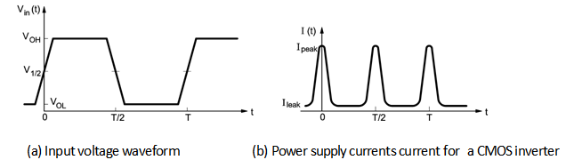
Fig2-Power-Delay-Product-in-CMOS