Home > Digital CMOS Design > CMOS Layout Design > Design Rule Check
CMOS-Layout-Design
Design Rule Check :
In order to ensure that none of the design rules are violated CAD tools named Design Rule Checking (DRC) is used. If DRC is not verified then it leads to the non functional design.
The layout rules are grouped in three categories that are transistor rules, contact and via rules and well and substrate contact rules.
Transistor rules :
The transistor can be created by overlapping the the active and polysilicon layers. The minimum length of transistor equals 0.24 m which is minimum width of polysilicon, whereas the width of the transistor is atleast 0.3 m which is the minimum width of active layer.
Figure below shows the layout of PMOS transistor.
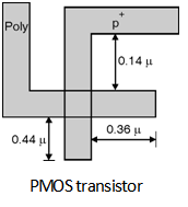
Fig1-Design-Rule-Check
Contact and Via rules :
A contact forms an interconnection between metal and active or polysilicon layer whereas via forms an interconnection between two metal lines. A contact or via is formed by overlapping the two interconnecting layers and provides a contact hole filled with metal between the two.
Figure below shows the contacts and via used in layout.
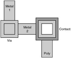
Fig1-Design-Rule-Check
Well and substrate contact rules :
For digital circuit design it is important for the well and substrate regions to be connected to the supply voltages. If this is not done then a resistive path is created between the substrate contact of the transistors and the supply rails which leads to parasitic effects such as latch up.