Home > Analog CMOS Design > MOSFET Fundamentals > Threshold Voltage
Threshold Voltage (VTH) :
Consider a n-channel MOSFET connected to external voltages as shown in Figure below, Here, VGS = 0 and drain, source and bulk are connected to ground, the drain and source are connected by back to back pn junctions i.e. Substrate-Source and Substrate-Drain junctions.
Therefore, both junctions have '0' V bias and considered OFF which results in very high resistance between drain and source. Further, the gate and substrate forms the plates of a capacitor with the gate oxide as dielectric.
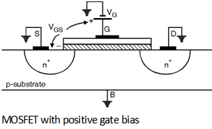
When a positive voltage is applied to the gate with respect to source the holes from the p substrate starts repelling from the gate area under oxide and leaves negative ions. So as to mirror the charge on the gate.
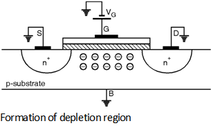
Hence, the positive gate leads to positive charge to accumulate on gate electrode and the negative charge to accumulate on the substrate which forms depletion region under gate. Under this condition no current flows because no charge carriers are available as shown in Figure below.
By increasing the gate potential surface inversion is starts and reaches the critical value at which n-type channel is created at the surface. When the gate potential is doubles the fermi potential (fF) strong inversion at the surface occures. The Fermi potential is expressed as,
fF = ln
Where K is Boltzmann's constant, NA is substrate doping and n i is intrinsic carrier concentration of silicon.
The increased gate voltage results in additional electrons in the thin inversion layer formed under the oxide. Hence a n-type channel is formed between the source and drain regions as shown in Figure below.
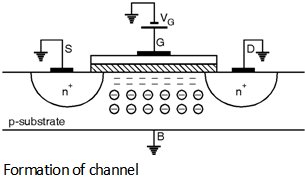
Thus, a 'channel' of charge carriers is formed under the gate oxide between source and drain terminals and the transistor is turned 'ON'. The value of gate voltage at which this phenomenon occurs is called as the threshold voltage (VTH). If VGS rises further the charge in the depletion region remains relatively constant while the channel charge density continuously increases and provides greater current from source to drain.
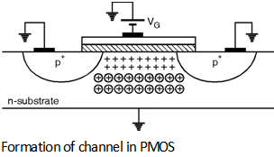
The turn ON phenomenon in a PMOS device is similar to that of NMOS transistor but with all the polarities reversed. If the gate-source voltage becomes sufficiently negative an inversion layer consisting of holes is formed at the oxide silicon interface providing a conduction path between the source and drain as shown in Figure below.
In semiconductor physics the threshold voltage (VTH) of a MOS transistor is defined as the gate voltage for which the oxide-substrate interface is inverted i.e. for NMOS transistor interface is n-type as substrate is p-type and for PMOS transistor interface is p-type as substrate is n-type.
From physics theory of NMOS transistor it is proved that the threshold voltage is given as :
VTH = VFB + 2 fF +
Where VFB is the flat band voltage given by,
VFB = fms -
Where fms is the difference between the work functions of the polysilicon gate and the silicon substrate.
Qf is the fixed charge due to surface states at the interface arise due to imperfections in the silicon-dioxide interface and doping. Cox is the oxide capacitance. fF is the Fermi potential defined in the Equation and Qdep is the charge in the depletion region given as :
Qdep =
Where,
ÃŽSi denotes the dielectric constant of Si.
Also, the term fms can be calculated as,
fms = -
Where Eg is the Bandgap energy of Si.