Home > Digital CMOS Design > CMOS Layout Design > Micron Design Rules
Micron-Design-Rules
Micron () Design Rules : Industry uses the micron design rules and code designs in terms of these micron dimensions. The micron design rules are as follows :
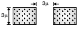
(1) Rules for N-well as shown in Figure below.
1. Width = 3
2. Space = 9
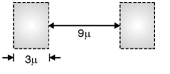
2) Rules for active area as shown in Figure below.
1. Minimum size = 3
2. Minimum spacing = 3
2. N+ active to N-well = 7
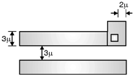
(3) Rules for poly 1 as shown in Figure below.
1. Width = 2
2. Spacing = 3
3. Gate overlap of active = 2
4. Field poly 1 to active = 1
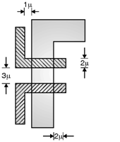
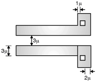
(4) Rules for contact to poly 1 as shown in Figure below.
1. Exact contact size = 2 2
2. Minimum poly overlap = 1
3. Minimum contact spacing = 2
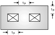
(5) Rules for contact to active as shown in Figure below.
1. Exact contact size = 2 2
2. Minimum active overlap = 1
3. Minimum contact spacing = 2
4. Minimum spacing to gate = 2
(6) Rules for metal 1 as shown in Figure below.
1. Width = 3
2. Spacing = 3
3. Overlap of contact = 1
4. Overlap of via = 2
 (7) Rules for metal 2 as shown in Figure below.
1. Width = 3
2. Space = 3
3. Metal 2 overlap of via = 2