Home > Digital CMOS Design > MOS Capacitor > Band Diagram of Nonideal MOS
Band Diagram of Nonideal MOS Structure at Equilibrium
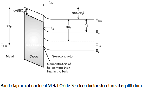
Consider the metal work function is greater than that of the semiconductor i.e. Φm > Φs.
The resulting band diagram of the structure is shown in Figure below.
In the band diagram, at semiconductor-oxide interface band bending occurs in the semiconductor side. This clearly shows the existence of electric field.
Hence the resulting electric field is directed from the semiconductor side to the metal side both in the semiconductor as well as across the oxide layer as shown in Figure below.