Home > Analog CMOS Design > MOSFET Fundamentals > Enhancement MOSFET Physical Structure
Enhancement MOSFET Physical Structure :
Figure below shows the simplified structure of the NMOS transistor. The NMOS transistor is fabricated on a p type substrate called as 'bulk' or 'body'. The two heavily doped n+ regions are diffused in the p type substrate which forms the source and drain terminals.
A heavily doped (conducting) piece of polysilicon which is simply called as poly is operates as a gate terminal. A thin layer of silicon dioxide (SiO 2) acts as insulating material between poly and substrate.
A junction formed between poly,SiO2 and substrate is called as MOS (metal-oxide-semiconductor) junction. The useful action i.e. formation of channel is occurred in the substrate region which is laying under the gate oxide. The structure is symmetric with respect to source and drain.
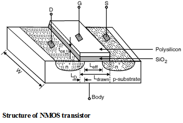
The dimension of the gate along the source drain path is called as the length 'L' and the dimension perpendicular to the length is called as width 'W' of the transistor.
The ratio of width to length is called as ratio which plays important role in digital designs.
During the fabrication of Source and Drain junction the dopants are “side diffuse†because of this the actual distance between source and drain is slightly less than 'L'.
Therefore Leff = Ldrawn - 2LD where L eff is effective length, Ldrawn is the total length and LD is the amount of side diffusion. The thickness of oxide t ox is the important parameter which decides the oxide capacitance Cox.
The principle thrust in MOS technology development is to reduce both L eff and tox from one generation to the next without degrading other device parameters.