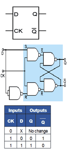
The major drawback of the SR flip-flop i.e. its indeterminate output and non-allowed logic states is overcome by the D type flip-flop. This flip-flop, shown in figure below with its truth table and a typical schematic circuit symbol. The D Flip-flop is called Data flip-flop because of its ability to ‘latch’ and remember data, or a Delay flip-flop because latching and remembering data which is used to create a delay in the progress of that data through a circuit. The simplest form of D Type flip-flop is basically a high activated SR type with an additional inverter to ensure that the S and R inputs cannot both be high or both low at the same time. This simple modification prevents both the indeterminate and non-allowed states of the SR flip-flop. The S and R inputs are now replaced by a single D input, and all D type flip-flops have a clock input.
Operation
As long as the clock input is low, changes at the D input make no difference to the outputs. The truth table in figure shows this as a ‘don’t care’ state (X). Whether the D input is active or not depends on the logic level of the clock input. Provided that the CK input is high (at logic 1), then whichever logic state is at D will appear at output Q and (unlike the SR flip-flops) Q is always the inverse of Q).
If D = 1, then S must be 1 and R must be 0, therefore Q is SET to 1.Alternatively, If D = 0 then R must be 1 and S must be 0, causing Q to be reset to 0.