The packaging is the major challenge to the IC designers. In packaging the pads are need to be connected to the IC internals and the surrounding blocks. In this case the IC engineer is responsible for designing all the assembly of the pad bonding. Therefore, here we will review packages and the problems involved in packaging. The necessary things involved in packaging are,
1. The package pins should have manageable solder connections.
2. The package provides the mechanical support to the chip
3. The packages should conduct the heat away from the IC to the surroundings.
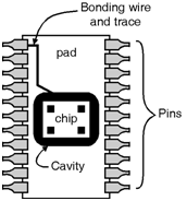
Figure below shows a schematic of a generic package. Here, the circuit board connects pins at the edge of the package. The pads are metal to be sol¬dered to the leads. The cavity is gold-plated to the IC sub¬strate. Packages also has electrical problems which are caused by the inductance of the pins and the printed circuit board attached to them-on-chip wires. Further, package inductance introduce significant voltage fluctuations.
 Fig_Off Chip Connections