Home > mini projects > 3 Bit Flash Type Analog to Digital Converter
3-Bit Flash Type Analog to Digital Converter
Abstract -A 3 bit analog to digital converter using comparators and priority encoder giving digital output is designed, and implemented using transistor-transistor logic and the subcircuits used for logic gates are implemented using CMOS logic.It is also called parallel ADC.
I. INTRODUCTION
» An analog-to-digital converter (A/D or ADC) produces a digital output (Bits) corresponding to an analog input voltage sample.
» Flash ADC Consists of a series of comparators, each one comparing the input signal to a unique reference voltage.
» The comparator outputs connect to the inputs of a priority encoder circuit, which produces a binary output.
II. DESIGN AND WORKING
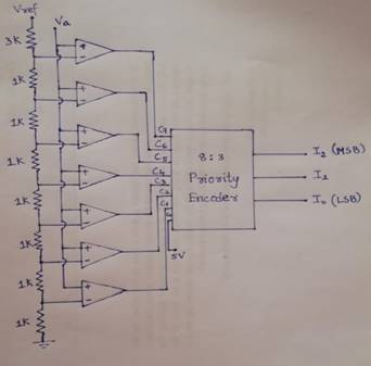
The circuit shown in figure takes the given analog signal as input (varying from 0-8v) and produces a digital output corresponding to the input given. In this circuit ,we used 7 comparators and a 8:3 priority encoder. There are 8 resistors for adjusting range and the reference voltage is taken as 10volts.
A. According to voltage division rule, voltage at 7th comparator will be Vref*(1k/10k) ie, 1V similarly at sixth comparator Vref*(2k/10k) ie, 2V. In this way all voltages will be divided as shown in table III.
B. Span is defined as the difference between maximum and minimum analog input voltages and here, it is 8v. step size is given by span/2^n where n is number of bits in the binary output(here, n=3). Hence, stepsize is 8/8=1.
C. The outputs of comparators are given as inputs to the priority encoder and the corresponding binary outputs are generated. The priority encoder generates a binary output based on the highest-order active input, ignoring all other active inputs. The output of the first comparator will be higher priority input compared to other bits
D. Here the input voltage Va is given to the non inverting terminal of the op amps and the voltage divided reference voltages are given to inverting terminal.For 1V < Va < 2v
7 th comparator output will be (Va-1) > 0 so logic 1 and for sixth comparator (Va-2) < 0 so logic 0. In this way we get 0000001 which will go to priority encoder input and the digital output will be 001.
III. INPUT RANGES AND CORRESPONDING OUTPUT
|
Input |
Priority |
Output |
Output |
Output |
|
|
Encoder |
|||||
|
Voltage |
MSB(18) |
||||
|
Input |
V(19) |
LSB(20) |
|||
|
Va V(9) |
|||||
|
0-1V |
00000001 |
0 |
0 |
0 |
|
|
1-2V |
00000011 |
0 |
0 |
1 |
|
|
2-3V |
00000111 |
0 |
1 |
0 |
|
|
3-4V |
00001111 |
0 |
1 |
1 |
|
|
4-5V |
00011111 |
1 |
0 |
0 |
|
|
5-6V |
00111111 |
1 |
0 |
1 |
|
|
6-7V |
01111111 |
1 |
1 |
0 |
|
|
7-8V |
11111111 |
1 |
1 |
1 |
|
V. FIGURES AND RESULTS
Digital Output (I2 I1 I0)
1) 000
2) 001
3) 010
4) 011
5) 100
6) 101
7) 110
8) 111
VI. CODES
*analog to digital
.include opamp.cir
.include spe.cir
r1 1 2 1k
r2 2 3 1k
r3 3 4 1k
r4 4 0 1k
x1 5 2 6 opamp
x2 5 3 7 opamp
x3 5 4 8 opamp
x4 6 7 8 9 10 11 prior
vr 1 0 dc 5
va 5 0 dc 1
v1 9 0 dc 5
.tran 1u 100us
.control
run
display
plot v(11)
set xbrushwidth=3
.endc
.end
SUBCIRCUITS :
*OP-AMP*
.subckt opamp 1 2 6
Rin 1 2 10Meg
E1 3 0 1 2 100k
R1 3 4 1k
C1 4 0 15u
E2 5 0 4 0 1
R2 5 6 10
.ends
*priority encoder
.include and4.cir
.include and3.cir
.include and2.cir.include or4.cir
.include or3.cir
.include ors.cir
.inlcude snot.cir
.subckt prit 8 7 6 5 4 3 2 1 9 10 11
x1 5 6 7 8 9 or4
x2 3 4 12 or
x3 6 13 not
x4 5 14 not
x5 13 14 12 15 and3
x6 8 7 15 10 or3
x7 7 16 not
x8 5 17 not
x9 3 18 not
x10 16 17 18 2 19 and4
x11 16 17 4 20 and3
x12 16 6 21 and2
x13 8 21 20 19 11 or4
.ends
*2 input and gate
.model MOSN NMOS
.model MOSP PMOS
.include snot.cir
.subckt and2 1 2 6
v3 3 0 dc 5v
M1 4 1 3 3 MOSP
M2 4 2 3 3 MOSP
M3 4 1 5 5 MOSN
M4 5 2 0 0 MOSN
x1 4 6 not
.ends
*3 input and
.model MOSN NMOS
.model MOSP PMOS
.include snot.cir
.subckt and3 1 2 3 8
V1 5 0 dc 5V
M1 4 1 5 5 MOSP
M2 4 2 5 5 MOSP
M3 4 3 5 5 MOSP
M4 4 1 6 6 MOSN
M5 6 2 7 7 MOSN
M6 7 3 0 0 MOSN
x1 4 8 not
.ends
*4 input and
.model MOSN NMOS
.model MOSP PMOS
.include snot.cir
.subckt and4 1 2 3 4 10
V1 6 0 dc 5v
M1 5 1 6 6 MOSP
M2 5 2 6 6 MOSP
M3 5 3 6 6 MOSP
M4 5 4 6 6 MOSP
M5 5 1 7 7 MOSN
M6 7 2 8 8 MOSN
M7 8 3 9 9 MOSN
M8 9 4 0 0 MOSN
x1 5 10 not
.ends
*or gate
.model MOSN NMOS
.model MOSP PMOS
.include snot.cir
.subckt or 1 2 6
V3 3 0 dc 5V
M1 5 1 3 3 MOSP
M2 4 2 5 5 MOSP
M3 4 1 0 0 MOSN
M4 4 2 0 0 MOSN
xinv1 4 6 not
*3 input or
.model MOSP PMOS
.model MOSN NMOS
.include snot.cir
.subckt or3 1 2 3 10
V1 5 0 dc 5v
M1 6 1 5 5 MOSP
M2 7 2 6 6 MOSP
M3 4 3 7 7 MOSP
M4 4 1 0 0 MOSN
M5 4 2 0 0 MOSN
M6 4 3 0 0 MOSN
x1 4 10 not
.ends
* 4 input or
.model MOSN NMOS
.model MOSP PMOS
.include snot.cir
.subckt or4 1 2 3 4 5
V1 6 0 dc 5v
M1 7 1 6 6 MOSP
M2 8 2 7 7 MOSP
M3 9 3 8 8 MOSP
M4 10 4 9 9 MOSP
M5 10 1 0 0 MOSN
M6 10 2 0 0 MOSN
M7 10 3 0 0 MOSN
M8 10 4 0 0 MOSN
x1 10 5 not
.ends
*not gate
.model MOSN NMOS
.model MOSP PMOS
.subckt not 1 2
M1 2 1 3 3 MOSP
M2 2 1 0 0 MOSN
Vd 3 0 DC 5V
.ends
MAIN CODE:
*flash type adc
.include opamp.cir
.include pri8.cir
r1 1 2 3k
r2 2 3 1k
r3 3 4 1k
r4 4 5 1k
r5 5 6 1k
r6 6 7 1k
r7 7 8 1k
r8 8 0 1k
x1 9 2 10 opamp
x2 9 3 11 opamp
x3 9 4 12 opamp
x4 9 5 13 opamp
x5 9 6 14 opamp
x6 9 7 15 opamp
x7 9 8 16 opamp
x8 10 11 12 13 14 15 16 17 18 19 20 prit
vr 1 0 dc 10v
va 9 0 dc 7.5v
v1 17 0 dc 5v
.control
tran 1u 2us
run
set xbrushwidth=3
set color0=white
set color1=black
op
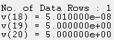
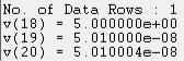
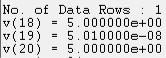
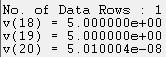
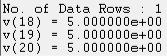
print v(18)
print v(19)
print v(20)
.endc
.end
VII. ADVANTAGES
Simplest of all analog to digital converters. Most efficient in terms of speed, very fast; limited only in terms of comparator and gate propagation delays.