Home > Analog CMOS Design > MOSFET Parasitics > Interconnect Resistance
Wire Parasitics :
The interconnects can be modelled as capacitive load or as a lumped or distributed RC network. If the interconnections lines are sufficiently long the rise times of the signal waveforms are large then the inductance also becomes important and in this situation the interconnection lines are modelled as transmission lines.
The interconnection delay becomes dominant factor in current VLSI chips. Thus it is important to discuss the interconnect parasitics and their effect on delay.
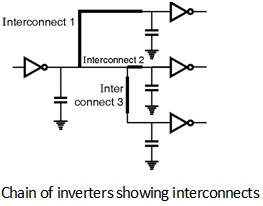
Figure below shows a simple situation where an inverter is driving three other inverters linked by inter connection lines of different length and geometry. If the load from each interconnection line can be approximated by a lumped capacitance then the total load seen by the primary inverter is simply the sum of all capacitive components.
The parasitic resistance of a metal or polysilicon creates significant effect on the propagation delay of signal flowing through the interconnect line.
The resistance of the interconnect depends on,
(1) The dimensions of the interconnect line.
(2) Type of material used.
(3) Locations of the contacts on line
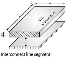
Consider the interconnection line shown in above Figure. The resistance in the wire is expressed as,
Rwire = r = Rsheet
Where r the resistivity of the interconnect material and Rsheet is the sheet resistivity in W/square.
Rsheet =
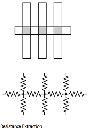
In order to extract the resistances from a layout, the abstraction of transistors has been connected by using the different nodes and the resistance is defined between pairs of points. Thus, a node attached to the terminals of k transistors gives rise to k(k − 1) /2 resistances.
Therefore, to reduce the number of resistances we must compute by chopping
the region into electrically isolated regions. If we add the appropriate k
− 2 junctions to a node attached to k terminals, then we need to compute
only k resistances, instead of
k (k − 2)/2.
Figure below shows a region which has eight terminals and 28 interconnection resistances. Thus, resistances can be more easily computed and shows that resistance extraction is the difficult and expensive problem. Indeed, most chips are manufactured without ever undergoing a complete resistance extraction because such an extraction would result in a prohibitively large network of resistors.