Home > Digital CMOS Design > Pass Transistor Logic
Pass-Transistor-Logic
Pass Transistor Logic :
The Pass transistor logic is required to reduce the transistors for implementing logic by using the primary inputs to drive gate terminals, source and drain terminals. In complementary CMOS logic primary inputs are allowed to drive only gate terminals.
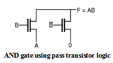
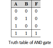
Figure below shows implementation of AND function using only NMOS pass transistors. In this gate if the B input is high the left NMOS is turned ON and copies the input A to the output F. When B is low the right NMOS pass transistor is turned ON and passes a '0' to the output F. This satisfies the truth table of AND gate reproduced in Table below for verification.

The major advantage of pass transistor logic is that fewer transistors are required to implement a given function. To illustrate this consider the implementation of AND gate using complementary CMOS logic. If we compare this with the same AND gate implementation using pass transistor logic the number of transistors required are four including the two transistor required to invert the input B. The another advantage of pass transistor logic is the lower capacitance because of reduced number of transistors. As discussed NMOS devices are effective in passing strong '0' but it is poor at pulling a node to VDD. Hence when the pass transistor pulls a node to high logic the output only changes upto VDD–VTh. This is the major disadvantage of pass transistors.

- 2-1-MUX-using-transmission-gate
- 4-1-multiplexer-using-CMOS-logic
- OR-gate-using-pass-transistor-logic
- Pass-Transistor-Logic
- Transmission-Gate
- XNOR-gate-using-pass-transistor-logic
- XOR-gate-using-pass-transistor-logic