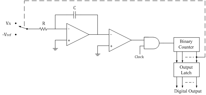
In dual slope type ADC, the integrator generates two different ramps, one with the known analog input voltage VA and another with a known reference voltage –Vref. Hence it is called a s dual slope A to D converter. The logic diagram for the same is shown below.
Operation:
The binary counter is initially reset to 0000; the output of integrator reset to 0V and the input to the ramp generator or integrator is switched to the unknown analog input voltage VA.
The analog input voltage VA is integrated by the inverting integrator and generates a negative ramp output. The output of comparator is positive and the clock is passed through the AND gate. This results in counting up of the binary counter.
The negative ramp continues for a fixed time period t1, which is determined by a count detector for the time period t1. At the end of the fixed time period t1, the ramp output of integrator is given by
∴VS=-VA/RC×t1
When the counter reaches the fixed count at time period t1, the binary counter resets to 0000 and switches the integrator input to a negative reference voltage –Vref.
Now the ramp generator starts with the initial value –Vs and increases in positive direction until it reaches 0V and the counter gets advanced. When Vs reaches 0V, comparator output becomes negative (i.e. logic 0) and the AND gate is deactivated. Hence no further clock is applied through AND gate. Now, the conversion cycle is said to be completed and the positive ramp voltage is given by
∴VS=Vref/RC×t2
Where Vref & RC are constants and time period t2 is variable.
The dual ramp output waveform is shown below.
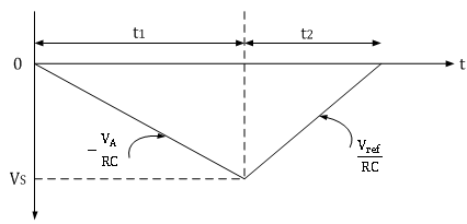
Since ramp generator voltage starts at 0V, decreasing down to –Vs and then increasing up to 0V, the amplitude of negative and positive ramp voltages can be equated as follows.
∴Vref/RC×t2=-VA/RC×t1
∴t2=-t1×VA/Vref
∴VA=-Vref×t1/t2
Thus the unknown analog input voltage VA is proportional to the time period t2, because Vref is a known reference voltage and t1 is the predetermined time period.
The actual conversion of analog voltage VA into a digital count occurs during time t2. The binary counter gives corresponding digital value for time period t2. The clock is connected to the counter at the beginning of t2 and is disconnected at the end of t2. Thus the counter counts digital output as
Digital output=(counts/sec) t2
∴Digital output=(counts/sec)[t1×VA/Vref ]
For example, consider the clock frequency is 1 MHz, the reference voltage is -1V, the fixed time period t1 is 1ms and the RC time constant is also 1 ms. Assuming the unknown analog input voltage amplitude as VA = 5V, during the fixed time period t1 , the integrator output Vs is
∴VS=-VA/RC×t1=(-5)/1ms×1ms=-5V
During the time period t2, ramp generator will integrate all the way back to 0V.
∴t2=VS/Vref ×RC=(-5)/(-1)×1ms=5ms=5000μs
Hence the 4-bit counter value is 5000, and by activating the decimal point of MSD seven segment displays, the display can directly read as 5V.