Field-programmable gate array (FPGA) uses logic block which is configurable. The term 'field-programmable’ shows that, that the device is programmable outside the foundry lab where it is manufactured. The internal architecture of an FPGA device consists of three parts, that are configurable logic blocks, the programmable interconnects and input/output blocks. Figure below shows
the architecture of a typical FPGA.
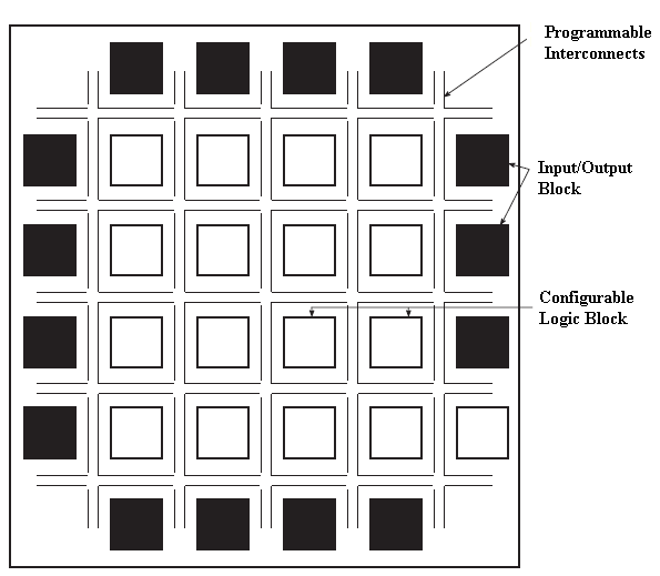
The Input/Output block provides bidirectional access to input/output pins of the FPGA package. The configurable logic block are not complex than the couple of logic gates or a look-up table. The programmable interconnects connect the configurable logic block to configurable logic blocks and also input/output blocks to configurable logic block.
FPGAs devices have higher logic density and larger performance as compared to other programmable logic devices. FPGA devices gives higher complexity equivalent to millions of gates. Further, FPGA has built-in hard-wired processors, large memory, clock management systems and support for many signalling technologies. FPGAs are used in processing and storage, digital signal processing, instrumentation and telecommunications system applications.
Since FPGAs program configuration is volatile, it requires bit RAM for storing the configured program.
Field Programmable Gate Array Quiz