Home > Digital CMOS Design > Propagation Delay > Parasitic Capacitances
MOSFET-Fundamentals
Parasitic Capacitances : As we know that, propagation delay of the CMOS inverter is determined by the time it takes to charge and discharge the load capacitor CL through PMOS and NMOS transistors respectively. Thus to have small propagation delay, CL should be as small as possible. So it is important to discuss the components of the load capacitance (CL ). Figure below shows the cascaded inverter pair along with the different parasitic capacitances in the circuit.
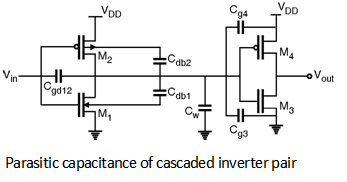
The various parasitic capacitances are : 1) Gate-Drain capacitance (Cgd12) 2) Diffusion capacitances (Cdb1, Cdb2) 3) Wiring capacitance (Cw) 4) Gate capacitances of fan-out (Cg3, Cg4)
The total load capacitance now is given as,
CL = (Cgd12 + Cdb1 + Cdb2 + Cg3 + Cg4 + Cw)
Note that the value of these capacitances in high to low and low to high transition may be different. In first order approximation we can assume that CLH L = CLL H.
In the previous sections we have seen that propagation delay of the CMOS inverter is determined by the time it takes to charge and discharge the load capacitor CL through PMOS and NMOS transistors respectively. Thus to have small propagation delay, CL should be as small as possible.