Home > Analog CMOS Design > MOSFET Parasitics > Interconnect Delay Model
Interconnect Delay Model :
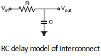
The simplest model which can be used to represent the resistive and
capacitive parasitics
of the interconnect line consists of one lumped resistance and one lumped
capacitance as shown in Figure below.
If the capacitance is discharged initially and the input signal is a step pulse at t = 0, then the output voltage waveform of the simple RC circuit can be given as,
Vout (t) = VDD
The rising output voltage reaches 50% point at t = tpLH .
Thus, V50% = VDD
and the propagation delay for this simple RC network is given as,
tpLH = 0.69 RC