Home > Digital CMOS Design > CMOS Layout Design > Stick Diagrams
Stick-Diagrams
Stick Diagrams :
A stick diagram is a kind of diagram which is used to plan the layout of a transistor cell. The stick diagrams uses "sticks" or lines to represent the devices and conductors.
Figure below shows the schematic of an inverter. In order to draw the layout of this circuit it is necessary to define the direction and metalization of the power supply, ground, input and output. The rules for drawing stick diagrams are :

Fig_Interconnect Routing Techniques
1) Power and ground lines run horizontally in metal 1.
2) The input and output are accessible from the top or bottom of the cell and will be in Metal 2 running vertically.
3) To draw the stick diagrams the conventions used in this book are shown in
Figure. These conventions are: For Metal-1 use thick solid line, for Metal-2 use thin solid line, for poly use thick dashed line, for active ( n+ or p+ ) use thin dashed line, for contact use "X" and for via use "O".
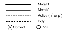
Fig-Stick-Diagrams