Home > mini projects > Regulated DC Power Supply using Series Voltage Regulator
Regulated Power Supply System Using
Series Voltage Regulator
Line regulation is the ability to maintain a constant output voltage level on the output channel of a power supply despite changes to the input voltage level. Line Regulation circuit is an essential component in the power supply for the devices requiring step-down of AC Mains Voltage. Voltage Regulators used for the same purpose have their applications in Adaptors, Computers and Alternators. In this work we demonstrate their working using Series Voltage Regulator.
I NTRODUCTION
Need for A Regulated Power Supply ?
Poor regulation as output voltage is not constant as load varies.
DC output voltage varies with the variations in the input voltage.
Load may have current sensitive devices which may get damaged due to unregulated voltage.
DC output voltage varies with temperature.
Block Diagram of a Regulated Power Supply
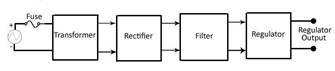
Transformer, Rectifier, Filter And Regulator are the basic components of any regulated power supply
A step-down transformer is used to step down the given voltage to desired value. The output magnitude of the transformer should be in a range that is compatible with the input voltage of the Regulator .
A Rectifier converts alternating current to direct current by allowing the current to flow through it one direction only.
Half Wave Rectifier, Full Wave Rectifier and Bridge Rectifier can be used. A bridge rectifier is used here since it is suitable for high voltage applications.
It has two diodes in series in each conduction path, the peak inverse voltage is equally shared by two diodes. Thus, it has less PIV rating per diode.
The current in both primary and secondary of the supply transformer flows for full cycle and hence for a given power output, power transformer of small size may be used in comparison with that in full-wave rectifier.
Output of a rectifier is pulsating in nature, it contains large ripple components. These ripple components are filtered by passing the output through a Filter. Filtering is usually done by shunting the load with a capacitor. A few filter circuits in common use are 1)Series Inductor Filter
2)Shunt Capacitor Filter
3)LC Filter
4)CLC or Pi filter
The working principle of shunt capacitor filter is that a capacitor stores energy when charging and delivers the energy to load while discharging. This process reduces the ripple components to a considerable extent.
Generally, fluctuations are observed in the Input Source Voltage. An extreme change in the output voltage may damage current sensitive devices at the load. Thus, Voltage Regulator is used to maintain a steady output voltage level inspite of the variations in the source voltage. Voltage Regulators may also include additional circuits for protection from short circuits and over-voltage protection.
Voltage Regulators can be broadly classified into two catagories asElectromechanical and Electronic Regulators. All electronic voltage regulators will have one Zener Diode as a source of stable voltage for Reference.
Zener Controlled Voltage Regulators can either have Transistor in series with Zener Diode or in parallel with Zener Diode.
A Discrete Transistor Series Voltage Regulator has a control element and Feedback element which help to maintain the steadiness of the output voltage.
Here we discuss Discrete Transistor Series Voltage Regulator.
BLOCK DIAGRAM FOR SERIES VOLTAGE REGULATOR
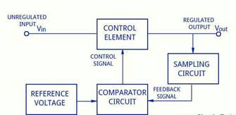
The sampling circuit collects a sample of the output voltage and uses it as a feedback signal to the comparator circuit.
The other input to the comparator circuit is the reference voltage.
Voltage Regulators generally use zener diode to provide constant source of voltage. The error voltage is generated at the output of the comparator block which drives the load current.
WORKING OF VOLTAGE REGULATOR
|
Component |
Value |
||
|
R1 |
930 ohm |
||
|
R2 |
1.57 K ohm |
||
|
R3 |
1.35 K ohm |
||
|
R4 |
1 K ohm |
||
|
D1 |
I= 20mA , V = 15V |
||
|
Tr2 (2N 930 ) |
Ic |
max=10mA, |
Vce |
|
max=45V |
|||
|
Table of Components |
|||
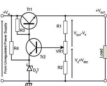
Tr1 is the series control element. It is a power transistor, mounted on a substantial heat sink to cope with the necessary power dissipation.
A stable reference voltage is provided by R4 & D1 from the un-regulated input voltage. Tr2 is the error amplifier and its gain is set by the value of load resistor R3. Tr2 compares the fraction of the output voltage VF fed back from the output potential divider R1/R2 with the stable reference voltage VZ across the zener diode D1.
We can write the output voltage equation as Vout = (Vz + V BE2) + (Vout - VF)
where,
Vz is the voltage across diode D1
VBE2is the base emitter voltage for Tr2
VF is the feedback voltage derived from potentiometer Vr1
Therefore, Vz + VBE2 is the voltage across Resistor R2 and lower part of Vr1
and Vout - VF is the voltage across R1 and upper part of Vr1.
If the feedback voltage VF is altered by adjusting Vr1 potentiometer, the difference between VF and Vz will change. This will cause a change in the error voltage controlling Tr1 and a change in the output voltage Vout.. The regulating action of the circuit is governed by the voltage across the base/emitter junction of Tr2, i.e. the difference between VF and Vz.
If VOUT tends to increase, then VF - V Z also increases. This increases the collector current of Tr2 and so increases the potential drop across R3 reducing the base voltage, and therefore the base/emitter voltage of Tr1, reducing the conduction of Tr1, so reducing current flow to the load.
The output voltage Vout is reduced in this way until a balance is reached, as the feedback portion (VF) of Vout is also reducing. The overall effect is that the output is maintained at a level, which depends on the proportion of feedback set by the variable resistor (part of R1/R2).
If the output voltage tends to decrease, then so does VF. The base/emitter voltage of Tr2 is reduced due to the stable V Z on the emitter. Tr2 conducts less and the current through R3 falls, reducing the potential difference across it. Tr1 base voltage rises, and increases the conduction of the control transistor. This increases output current and VOUT until VF is once more at the correct level.
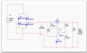
To design a regulated power supply to provide output voltage of 25V from AC source input of 50V, 50Hz frequency. Supply load current I(L) < 1A.
CALCULATIONS
(subscripts 1 and 2 correspond to Transistor1 and 2 parameters)
The Zener diode provides Vr = 15V at Iz = 20mA IC2= I E2= 10mA
The Q2 Transistor can provide the collector current of 10mA. For this transistor the manufacturer specifies ICmax= 10mA and V CE max= 45V
At IC2 = 10mA, the following parameters were measured
hfE2=220 , hfe2 = 200 , hie2 = 800
ID= 10mA
R4 = (Vo-Vr)/ ID = (25-15)/10 = 1K
IB2 = IC2 / hFE2 = 10mA/220 = 45uA
V2 = VBE2 + Vr = 15.7V0
R1 = Vo-V2/ I1 = 930 ohm
R2 = V2/ I1 = 1.570 k ohm
The Transistor Q1 we measure at IC1 = 1A hfE1=125 , hfe1 = 100 , hie1 = 20
We thus have
IB1 =( ID + I1 + IL )/h fE1 = (1000+10+10)/125 = 8mA
The Current I through the resistor R3 is I = IB1 + I C2 = 8+10 =18mA
The Value of R3 corresponding to Vi= 45 and to IL = 1A is given by
R3 = (Vi-(VBE1+Vo))/I = (50-25.7)/18 x e-3 = 1.350 k ohm
The Circuit is simulated on NG-spice using the values of given parameters and the following observations are done
CONCLUSIONS
The Circuit is simulated successfully in Ngspice and we get smooth DC output voltage.
The potential division can be made variable by using the potentiometer VR1 and we can adjust the output voltage to the required value.
The potential divider reduces feedback loop gain and thus reduces the regulation performance. Generally there is sufficient loop gain for this not to be a major problem except only when a very small proportion of the output is sampled.