Home > mini projects > DESIGN OF OP AMP USING CMOS WITH IMPROVED PARAMETERS

DESIGN OF OP-AMP USING CMOS WITH IMPROVED PARAMETERS
Abstract
In this project, a comparative analysis of two stage conventional operational amplifier and proposed design of operational amplifier using CMOS technology has been carried out to enhance the bandwidth ,slew rate and the gain of the device.The results of this implementation show that the gain has been improved by 27dB, Unity gain frequency by 64 times and Slew rate by 8 times.
Project Description:
There are various parameters to be considered while designing any circuit. The parameters that are to be considered when designing an Op-Amp are described below.
1. Gain: The most important factor in designing an Op-Amp circuit is the required gain from the circuit. In this circuit, we expect a gain of >= 60 dB. In order to achieve such higher gains, we use multiple stage CMOS Op-Amp. For this project we use 2 stage op-amp with differential amplifier at the first stage and a common source amplifier at 2nd stage
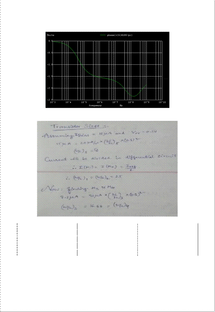
2. Unity Gain Frequency: The frequency at which the Gain of the circuit becomes '1' or 0 dB is termed as Unity Gain Frequency. In this project, we need Unity Gain Frequency to be greater than or equal to between phase measured in degrees for an output signal and 180 degrees. Phase margin should be >= 45 degrees.
3. Slew Rate: It is maximum rate of change of output with respect to unit
time. In this project, we expect slew rate to be greater than or equal to 80 V/us.
Explanation
The circuit contains two stages. The first is formed by the differential pair Q1-Q2 with its current mirror load Q3-Q4. Differential pair is biased using the current source Q5. The transistor Q5 is fed by a reference current mirror IRef. The second stage is comprised of transistor Q6 with its current source load Q7. The second stage is used to improve the gain significantly.
The two stage Op-Amp is expected to produce a gain greater than 1000. In order to design the Op-Amp with the specifications mentioned above,
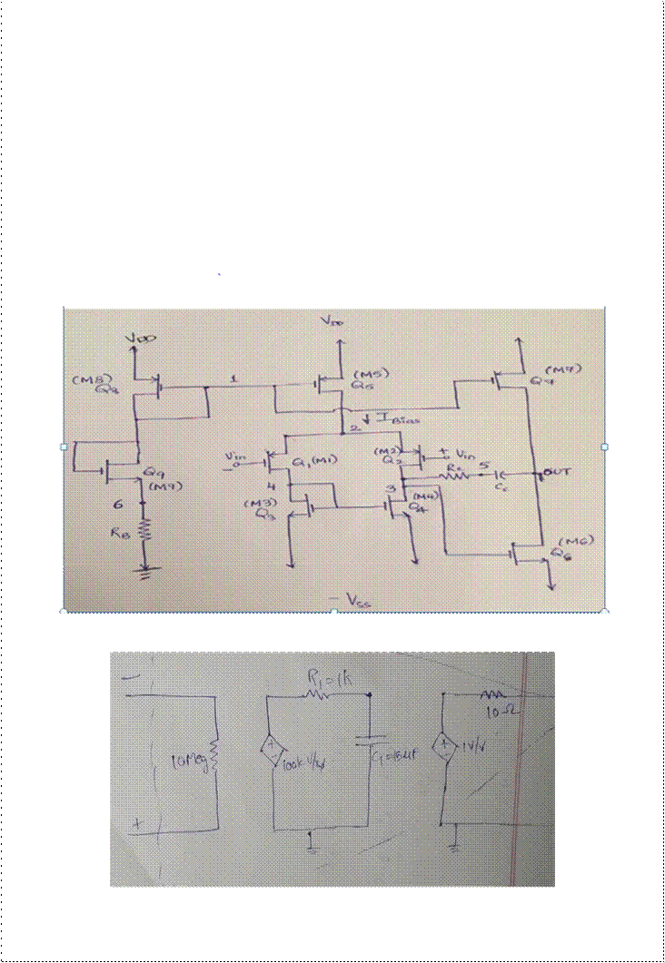
the first step is to estimate the value ofbias current from current source IRef. The next step is to calculate the (W/L) ratios of the transistors in the circuit based on the Reference Current.
Finally, we estimate the value of the compensation Capacitor required to provide the negative feedback. In order to avoid systematic output dc offset voltage, we need to choose the (W/L) ratios of transistors carefully.
Design Specifications
Gain >= 60 dB, Unity Gain frequency >= 60MHz, Slew Rate >= 80 V/us. The power supply is +/-7.5V
SCHEMATIC DIAGRAM
EQUIVALENT CIRCUIT OF CONVENTIONAL OP AMP
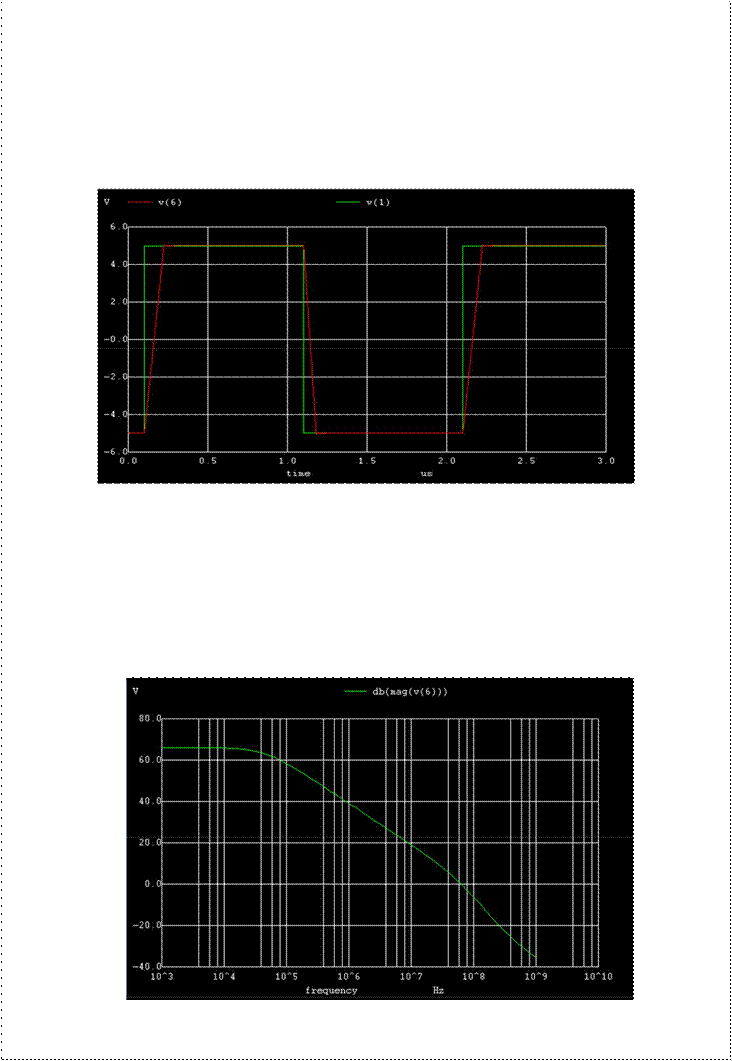
The transient simulation is the calculation of a networks response on arbitrary excitations. The results are network quantities (branch currents and node voltages) as a function of time. Substantial for the transient analysis is the consideration of energy storing components, i.e. inductors and capacitors.
AC ANALYSIS
The AC analysis is a small signal analysis in the frequency domain. Basically this type of simulation uses the same algorithms as the DC analysis . The AC analysis is a linear modified nodal analysis. Thus no iterative process is necessary.
MAGNITUDE PLOT:
INITIAL HAND CALCULATIONS :-
Comparative analysis of the two Operational Amplifiers
|
Parameter |
Conventional op-amp |
Proposed op-amp |
||
|
Gain |
40 dB |
67 dB |
||
|
Unity gain frequency |
1 Mhz |
64 Mhz |
||
|
Slew rate (rise) |
11.184 V/us |
81.16 V/us |
||
|
Slew rate(fall) |
-9.7894 V/us |
-124.57 V/us |
||