Home > mini projects > AMPLITUDE MODULATION AND DEMODULTION USING BJT AMPLIFIER AND DIODE DETECTOR
AMPLITUDE MODULATION AND DEMODULTION USING BJT AMPLIFIER AND DIODE DETECTOR
Abstract-This project explores the robust design of amplitude modulation and demodulation using BJT Amplifier and Diode detector
.Considering the difficulties faced by the designer in terms of hardware for designing such systems we have used a system that uses less hardware for this process.We have written the ngspice code for the modulator and demodulator as per the circuit diagram and simulated it in ngspice.
1. INTRODUCTION
In the earlier days amplitude modulation was the simplest technique used for transmission of analog signals. The major advantage that got the designers attention was the simplicity associated with it. Another main important advantage regarding amplitude modulation was that it can transmit signal/message/wave over long distance. So radio channels which are transmits signal worldwide like vividh bharti also uses amplitude modulation. There are different types of amplitude modulation like DSB-FC,SSB, SSB-SC,DSB-SC,VSB.
Here we have done simulation using DSB-SC .We have suppressed carrier because carrier doesn't carry any information instead consume power.SSB-SC and VSB are the improvement in DSB-SC as they don't carry carrier with them hence requires less power. They also requires less band width.
2. MODULATOR DESIGN Modulator:
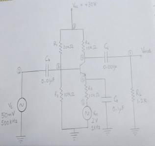
Fig.1-circuit of amplitude modulator
Modulation is defined as the process by which some characteristics of a carrier signal isvaried in accordance with a modulating signal. The base band signal is referred to as the modulating signal and the output of the modulation process is called as the modulation signal. Amplitude modulation is defined as the process in which is the amplitude of the carrier wave is varied about a means values linearly with the base band signal.
The envelope of the modulating wave has the same shape as the base band signal provided the following two requirements are satisfied
1. The carrier frequency fc must be much greater then the highest frequency components fm of the message signal m
(t) i.e. fc >> fm
2. The modulation index must be less than unity. if the modulation index is greater than unity, the carrier wave becomes over modulated.
Calculations:
Amax=785mV
Amin=511mV
Modulation index (µ)= + − = .2114
![]()
Since µ<1, we can obtain the message signal after demodulation without any loss of information.
Working:
Here we have used Double Side Band Carrier (DSB-C) for modulation purposes.
Source called Vm generates the message to be transmitted. It's amplitude is 2V and frequency is 1kHz. The circuit's working principle is as follows: As we can see we have a simple common emitter amplifier topology because of the bypass capacitor Cb connected to the emitter of the transistor, as far as the small signal operation is considered. But the thing is, because we connected the message signal to the branch by-passed by a capacitor, we constantly change the biasing point of the transistor according to our message signal. So we can say that we have a variable gain since the trans conductance of transistor varies. Then we high-pass filter it with the capacitor Cc.
3.DEMODULATOR DESIGN
Demodulator:
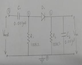
Fig.2 -demodulation circuit
The process of detection provides a means of recovering the modulating Signal from modulating signal.
Demodulation is the reverse process of modulation. The detector circuit is employed to separate the carrier wave and eliminate the side bands. Since the envelope of an AM wave has the same shape as the message, independent of the carrier frequency and phase, demodulation can be accomplished by extracting envelope.
The depth of modulation (modulation index) at the detector output greater than zunity(µ>1) and circuit impedance is less than circuit load (Rl > Zm) results in clipping of negative peaks of modulating signal. It is called "negative clipping ".
To understand it, we may divide it into two blocks:
-Main Envelope detector; an half wave rectifier with a filter capacitor (diode D1, resistor R2 , capacitor C2)
-An high pass filter (capacitor C1, resistorR1)
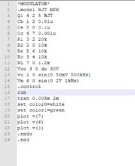
Main envelope detector: NGSPICE MODULATOR CODE:
With diode D1 and the resistor R2 we half wave rectify the signal. Then with the filter capacitor we try to follow the envelope of the signal. The crucial point when designing this circuit is that we have to choose RC time constant so that, it is not too small to avoid excessive discharges between peaks, and we don't have to choose it too large, to make it possible for the capacitor to follow the signal.
To summarize here is the interval in which we have to choose the RC time constant:
1/ωc << RC < 1/(2πB) where B is the bandwidth of the message signal. Since we have used single tone message signal we can replace B by fm. So let us do the calculation:
0.318us<<RC <0.159ms
We chose RC as:
|
100k ohm*0.001uF = 0.1ms |
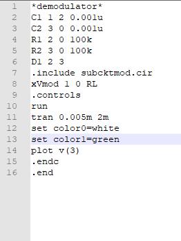
NGSPICE DEMODULATOR CODE: |
||||
|
Table1:Values of Various components |
|||||
|
involved in modulator design : |
|||||
|
Symbols |
Components |
Calculated values |
|||
|
Vcc |
Power supply |
30V |
|||
|
Vc |
Carrier |
500khz,50mV |
|||
|
Vm |
Messege |
1khz,2V |
|||
|
Ib |
Base current |
12uA |
|||
|
Ie |
Collector current |
1.2mA |
|||
|
R1 |
Pot.divider |
resistance1 |
20k ohm |
||
|
R2 |
Pot. divider |
resistance1 |
10k ohm |
||
|
Re |
Emitter resistance |
10k ohm |
|||
|
Cb |
Coupling Capacitor |
0.01uF |
|||
|
Cc |
Coupling Capacitor |
0.001uF |
|||
|
Ce |
Bypass capacitor |
0.1uF |
|||
SIMULATION OUTPUTS:
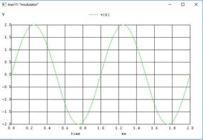
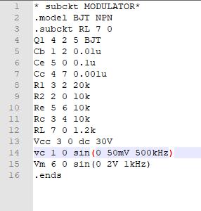
Fig.3-messege signal(input to modulator)
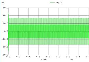
Fig.4-carrier wave (input to modulator)
Fig.5-modulated signal (output of modulator)
The output is as expected envelope of modulating signal
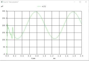
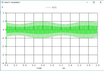
Fig.6- demodulator output(reconstructed input)
4.CONCLUSION AND DISCUSSION
The demodulator output is close replica of modulating signal with some approximations considering the noise and limitations of hardware in receiver and transmitor.