Home > Analog CMOS Design > Signal Conditioning > ADC Circuits
Analog to Digital Circuits :
There exists number of A/D converter circuits varying in complexity and speed. In this section we will discuss four different approaches that are :
1) Simple feedback type ADC
2) Dual slope ADC
3) Parallel or Flash ADC
4) Charge Redistribution converter.
Figure below shows a simple ADC that employs a comparator, one up/down counter and DAC. The comparator circuit provides an output that assumes one of two distinct values, positive when the difference input signal is positive and negative when the difference input signal is negative. An up/down counter is simply a counter that can count either up or down depending on the binary level applied at its up/down control terminal. As DAC is employed in the feedback loop it is usually called feedback type ADC.
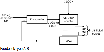
In order to discuss the operation of this ADC consider initially counter is reseted to '0'. Hence the DAC output is 0 and the output of comparator will be high which instructs the counter to start up counting. As the count increases the output of DAC rises. The process continues until the DAC output reaches the value of the analog input signal at this point the comparator switches and stops the counter.
The counter output will be the digital equivalent of the input analog voltage.
Dual-Slope ADC :
Figure below shows the circuit of dual slope ADC. This type of circuit has very high resolution in the order of 12 to 14 bit. But this conversion is slow.
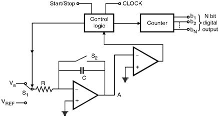
The operation of the dual slope ADC is explained in two phases. In phase I we assume that the analog input signal Va is negative prior to the start of conversion cycle, switch S2 is closed thus the capacitor C is discharged and makes the voltage at Node A zero. The conversion cycle begins with opening S2 and connecting integrator input through switch S1 to the analog input signal. As the analog input signal is negative a current I = will flow through R in the direction away from the integrator. Thus, the voltage at node A rises linearly with slope of = as shown in Fig. 6.13.3. Simultaneously the counter is enabled and it counts pulses from a fixed frequency clock. This phase of the conversion process continues for a fixed duration T 1. It ends when the counter has accumulated a fixed count denoted by NREF. Usually for an N bit converter NREF = 2N, at the end of phase the counter is reset to zero.
Phase II of conversion begins at t = T1 by connecting integrator input through switch S1 to the positive reference voltage V REF. The current into the integrator reverses direction and is equal to . Thus the voltage at node a decreases linearly with a slope of . Simultaneously the counter is enabled and it counts the pulses from the fixed frequency clock. When the voltage at node A reaches zero volts, the comparator signals the control logic to stop the counter. Denoting the duration of phase II by T2.
As the counter reading NREF at the end of T1 is proportional to T1 and the reading n at the end of T2 is proportional to T2, we get,
n = NREF
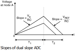
Thus, the content of the counter, 'n' at the end of the conversion process is the digital equivalent of Va applied at input of ADC.
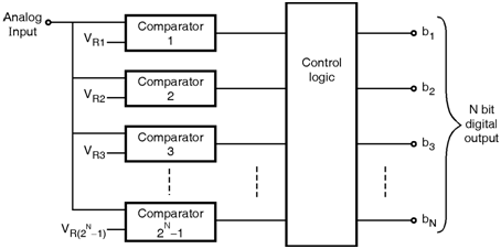
The fastest ADC scheme is the parallel or flash conversion process shown in
Figure below. This scheme utilizes 2N - 1 comparator to compare
the input signal level with each of the
2N - 1 possible quantization levels. The outputs of the
comparator are processed by an encoding logic block to provide the N bits
of the output digital word. The complete conversion in this process is
obtained in one clock cycle.
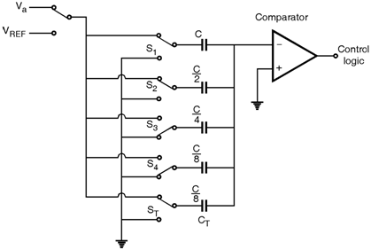
Charge Redistribution ADC :
This technique is suited for CMOS implementation of the ADC. As shown in Fig. 6.13.5 the circuit uses a binary weighted capacitor array, a voltage comparator and analog switches and control logic to switch the switches. The circuit shown is a 4 bit converter. A capacitor CT serves the purpose of terminating capacitor array making the total capacitance equal to desired value of 2C. The accuracy of this method is independent of the value of stray capacitances from bottom plate of the capacitors to ground because the bottom plates are connected either to ground or to V REF. Thus the charge on the stray capacitances will not flow into the capacitor array.