CMOS (complementary metal-oxide-semiconductor) technology is used predominantly to create digital circuitry. The fundamental building blocks of CMOS circuits are P-type and N-type MOSFET transistors. A P-type MOSFET can be modeled as a switch that is closed when the input voltage is low (0 V) and open when the input voltage is high (5 V). A N-type MOSFET can be modeled as a switch that is closed when the input voltage is high (5 V) and open when the input voltage is low (0 V). The basic idea for CMOS technology is to combine P-type and N-type MOSFETs such that there is never a conducting path from the supply voltage (5 V) to ground. As a consequence, CMOS circuits consume very little energy. CMOS technology employs two types of transistor: n-channel and p-channel. The two differ in the characteristics of the semiconductor materials used in their implementation and in the mechanism governing the conduction of a current through them. We will model this behavior using switches controlled by voltages corresponding to logic 0 and logic 1. Such a model ignores complex electronic devices and captures only logical behavior.
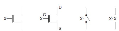
The symbol for an n-channel transistor is shown in Figure below . The transistor has three terminals: the gate (G), the source (S), and the drain (D). The voltage applied between G and S determines whether a path for current to flow exists between D and S. If a path exists, we say that the transistor is ON, and if a path does not exist, we say that the transistor is OFF. The n-channel transistor is ON if the applied gate-to-source voltage is H and OFF if the applied voltage is L. Here we will make the usual assumption that a 1 represents the H voltage range and a 0 represents the L voltage range. The notion of whether a path for current to flow exists is easily modeled by a switch. The switch consists of two fixed terminals corresponding to the S and D terminals of the transistor. In addition, there is a movable contact that, depending on its position, determines whether the switch is open or closed. The position of the contact is controlled by the voltage applied to the gate terminal G. Since we are looking at logic behavior, this control voltage is represented on the symbol by the input variable X on the gate terminal. For an n-channel transistor, the contact is open (no path exists) for the input variable X equal to 0 and closed (a path exists) for the input variable X equal to 1. Such a contact is traditionally referred to as being normally open, that is, open without a positive voltage applied to activate or close it.
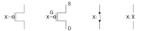
The symbol for a p-channel transistor is shown in Figure bolow. The positions of the source S and drain D are seen to be interchanged relative to their positions in the n-channel transistor. The voltage applied between the gate G and the source S determines whether a path exists between the drain and source. The negation indicator or bubble appears as a part of the symbol. This is because, in contrast to the behavior of an n-channel transistor, a path exists between S and D in the p-channel transistor for input variable X equal to 0 (at value L) and does not exist for input variable X equal to 1 (at value H).
This behavior is represented by the model which has a normally closed contact through which a path exists for X equal to 0. No path exists through the contact for X equal to 1.
The popular CMOS family include,
4000A,
4000B,
4000UB,
54/74C,
54/74HC,
54/74HCT,
54/74AC
54/74ACT
The 4000A CMOS family has been replaced by its high-voltage versions in the 4000B and 4000UB CMOS families, with the former having buffered and the latter having unbuffered outputs. 54/74C, 54/74HC, 54/74HCT, 54/74AC and 54/74ACT are CMOS logic
families with pin-compatible 54/74 TTL series logic functions.
CMOS QUIZ:
CMOS Family