Home > mini projects > AMPLITUDE MODULATION AND DEMODULATION
AMPLITUDE MODULATION AND DEMODULATION
Abstract -A single tone sinusoidal signal is transmitted using AMPLITUDE MODULATION and is demodulated at the receiver's end using an ENVELOPE DETECTOR and the attenuated signal is amplified using COMMON SOURCE BJT AMPLIFER.
I. INTRODUCTION
Modulation is used in efficient radiation of signals. This way, the antenna size can be made small as well as more than one signals can be transmitted through a single channel by transmitting modulating signals at different frequency bands. Amplitude modulation implies variation in the amplitude of the carrier signal according to the amplitude of the modulating signal. Special circuits are required in the receiver to reduce the effects of communication channel and demodulate the modulated signal to receive the message signal. Further, in oreder to improve the power of the message signal, mosfet amplifier is used to amplify the voltage level and
II. DESIGN AND WORKING
The amplitude modulation and demodulation technique involved in this project comprises of three stages:
(1) Modulation using common emitter amplifier
Amplitude modulation is defined as the process in which is the amplitude of the carrier wave is varied about a means values linearly with the base band signal. The envelope of the modulating wave has the same shape as the base band signal provided the following two requirements are satisfied
1. The carrier frequency fc must be much greater then the highest frequency components fm of the message signal m (t) i.e. fc >> fm
2. The modulation index must be less than unity. if the modulation index is greater than unity, the carrier wave becomes over modulated.
FIG.1.1 Common Emitter Transistor
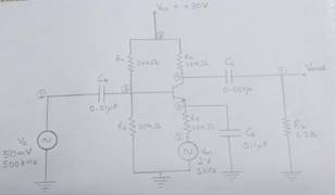
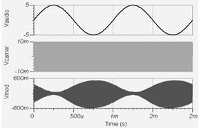
FIG 1.2 Message, Carrier signal, Modualted Signal
The high frequency carrier signal is applied on the coupling capacitor. The coupling capacitor is used to separate the AC signal from the DC biasing voltage.
The resistors R1 and R2 are used to set up a good Q-point stability of the transistor.
When an emitter resistance is added in a CE amplifier, its voltage gain is reduced but the input impedance increases. When a bypass capacitor is connected in parallel with an emitter resistance, voltage gain of CE amplifier increases.
As we connected the message signal to the branch by-passed by a capacitor, we constantly change the biasing point of the transistor according to our message signal. So we can say that we have avariable gain since the transconductance of transistor varies.
Modulated signal:
s(t) = Ac(1+ka*m(t))cos(2*Ï€*fc*t)
Calculations: (For Vm= 2v) Amax = 650mV
Amin = 615mV
Modulation Index(µ) = (Amax-Amin)/(Amax+Amin)
= 0.02767
Since µ<1, we can obtain the message signal after demodulation without any loss of information.
(2) Demodulation using Envelope Detector
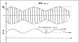
The process of detection provides a means of recovering the modulating Signal from modulating signal. Demodulation is the reverse process of modulation. The detector circuit is employed to separate the carrier wave and eliminate the side bands.
Since the envelope of an AM wave has the same shape as the message, independent of the carrier frequency and phase, demodulation can be accomplished by extracting envelope. An increased time constant RC results in a marginal output follows the modulation envelope. A further increase in time constant the discharge curve become horizontal if the rate of modulation envelope during negative half cycle of the modulation voltage is faster than the rate of voltage RC combination ,the output fails to follow the modulation resulting distorted output is called as diagonal clipping : this will occur even high modulation index.
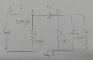
FIG2.2 Demodulated Output
With diode D1 and the resistor R2, we half wave rectify the signal. Then with the filter capacitor we try to follow the envelope of the signal. The crucial point when designing this circuit is that we have to choose RC time constant so that, it is not too small to avoid excessive discharges between peaks, and we
don't have to choose it too large, to make it possible
for the capacitor to follow the signal. To summarize, here is the interval in which we have
to choose the RC time constant: 1/ωc < < RC < 1/(2πB) where B is the bandwidth of the message signal. Since we have used single tone
|
message |
signal we |
can |
replace |
B by fm. |
|||
|
So |
let |
us |
do |
the |
calculation: |
||
|
0.318us<<RC<0.159ms |
|||||||
|
We chose RC as 100k |
ohm * 0.001uF = 0.1 ms . |
||||||
|
So we satisfied the constraint. |
|||||||
(3) COMMON SOURCE MOSFET AMPLIFER
Metal-Oxide-Silicon FET, or MOSFET for short, is an excellent choice for small signal linear amplifiers as their input impedance is extremely high making them easy to bias. But for a mosfet to produce linear amplification, it has to operate in its saturation region, unlike the Bipolar Junction Transistor. But just like the BJT, it too needs to be biased around a centrally fixed Q-point.
FIG2.1 Envelope Detector
FIG3.1 MOSFET AMPLIFIER
- The demodulated output is passed throught the
common source MOSFET amplifier and the power of
the received message signal is increased.
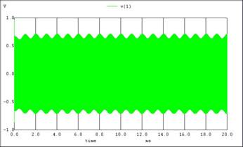
GRAPH1.1 Modulated Waveform
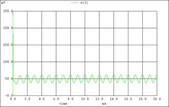
GRAPH1.2 Envelope Detector Output
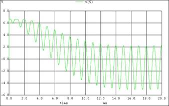
GRAPH1.3 Amplified Output
IV.CODES
(A)MODULATOR SUBCIRCUIT
*modulator
.subckt modulator 7
Vc 1 0 sin(0 50m 500k)
Vm 6 0 sin(0 5 1000)
Vcc 3 0 dc 30
R1 3 2 20k
R2 3 0 10k
Rc 3 4 10k
Re 5 6 10k
Cb 1 2 .01u
Cc 4 7 .001u
Ce 5 0 .1u
Rl 7 0 1.2k
.model bjt npn
Q1 4 2 5 bjt
.ends
(B) MOSFET AMPLIFIER SUBCIRCUIT * mosfet amplifier
.subckt mosf 5 6
Vdd 1 0 dc 15
R1 1 3 200k
R2 3 0 100k
Rd 1 2 470
Rs 4 0 150
Rl 6 0 10k
.model mosfet nmos(VTO=2 Kp=50e-3 Cbd 120p Cbs=120p)
M1 2 3 4 0 mosfet
C1 5 3 10u
C2 2 6 10u
Ce 4 0 320u
.ends
(C )Demodulator Circuit
*demodulator
.include modulator.cir
X1 1 modulator
C1 1 2 0.001u
C2 3 0 0.001u
R1 2 0 100k
R2 3 0 100k
D1 2 3
.include mosfetAmplifier.cir
X2 3 4 mosf
X3 4 5 mosf
.tran 1u 20m
.control
run
display
set color0 = white
set color1 = black
plot v(1)
plot v(3)
plot v(5)
.endc
.end