Home > mini projects > SCHMITT TRIGGER USING 555
Abstract - Schmitt trigger is an electronic circuit,which acts as a comparator ,that is used to detect a given reference level.It has two stable states logic 1,logic 0.Whenever the input is sine,triangle,or any periodic waveform the output of the schmitt trigger come out to be a rectangular or square wave form which has sharp edges.The advantage of the schmitt trigger is the desirable rise and fall times for all digital circuits.In this project,the design and implementation of schmitt trigger using 555timer is implemented.
IndexTerms- Comparator,digital circuits, 555 timer,rectangular waveform,Schmitt trigger
I.INTRODUCTION
The schmitt trigger is called as squaring circuit,as it convert any shape of input waveform to a square wave.The output voltage changes its state everytime when the input voltage crosses the threshold voltage.The input voltage at which the output switches from +Vsat to -Vsat is called the upper triggering point or upper trip point(U.T.P),in the sameway the input voltage at which output switches from -Vsat to +Vsat is called lower triggering point or lower trip point(L.T.P).
The difference between U.T.P and L.T.P is known as hysterisis voltage(Vh) and is also called as deadzone of schmitt trigger.In other words hysteresis is also defined as lagging of the lower threshold voltage from the upper threshold voltage.If Vh is large,then the circuit would never reset itself, once it has responded to a transition.
The rest of the project consists of following sections:section II decsribes schmitt trigger overview,section III focuses on the system design,results and discussions are reported in section IV.
II.SCHMITT TRIGGER OVERVIEW
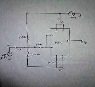
The following circuit shows the structure of 555 timer used as schmitt trigger.
Pins 4 and 8 are connected to the supply (Vcc).The pins 2 and 6 are shorted and input is given to this common point through the capacitor.This common point is supplied with an external bias voltage Vcc/2 with the help of voltage divider circuit formed by resistors R1 and R2.
The output retains its values when the input is between the two threshold values is called Hysterisis and the Schmitt trigger acts as a memory element.
The threshold values in this case are 2/3Vcc and 1/3Vcc,i.e.the upper comparator trips at 2/3Vcc and the lower comparator trips at 1/3Vcc.The input voltage is compared to this threshold values by the individual comparators and the flipflop is set or reset accordingly.Based on this the output becomes high or low.
Consider an example:When a sinewave of amplitude greater than Vcc/6 is applied at the input the flipflop is set and reset alternately for the positive cycle and the negative cycle.The output is a square wave and the waveforms for input sinewave are shown below.
III.SYSTEM DESIGN
This system is designed using 555 timer IC.A 555 timer is an integrated circuit used in variety of timer,pulse generation and oscillator application.It is used to provide time delays,as an oscillator and as a flipflop element.
Basic theory of operation :
When the trigger voltage goes below 1/3Vcc (its reference voltage)the comparator sets the flipflop,which pulls the output high and turns off the discharge.when the threshold swings higher than 2/3Vcc(its reference voltage) the comparator resets the flipflop,which pulls the output low and turns discharge on.
This basic operation allows 555 timer to operate in various phase with different modes.
The internal block diagram and schematic of 555 timer are highlighted with some colour to clarify how the chip is implemented.
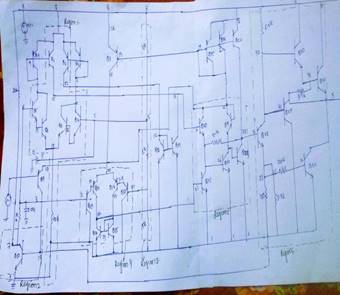
RegionIII: Between the positive supply voltage Vcc and ground, a voltage divider consisting of 3 identical register which create two reference voltages at 1/3Vcc and 2/3 Vcc.All three resistors have same resistance of 5kohm.
Region I: The comparator negative input is connected to high reference voltage divider of 2/3Vcc and comparator positive input to threshold pin.
RegionIV: This region stores the state of the timer and is controlled by two comparators.
RegionVI: This region is a stage with push-pull output driver that can load the output pin with upto 200mA.
RegionII: This region turns on the transistor that connects the discharge pin to ground.
RegionIV: The comparator positive input is connected to the lower reference voltage divider of 1/3Vcc and the comparator negative input is connected to the trigger pin.
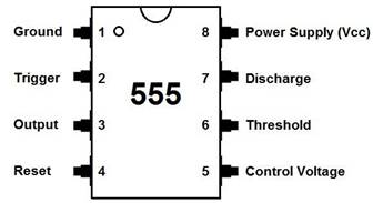
PIN CONFIGURATION OF 555:
PIN1: Ground reference voltage.
PIN2: Trigger
TRIGGER: When the voltage at this pin falls below ½ of control pin voltage(1/3Vcc),the output pin goes high and a timing interval starts.As long as this pin continued to be kept at low voltage,the output will remain high.
PIN3: Output pin.
PIN4: Reset
A timing interval may be reset by driving this pin to ground.But the timing does not begin again until this pin rises above 0.7V.
PIN5: Control Voltage input
This pin provides control access to the internal voltage divider.By applying a voltage to the control voltage input,one can alter the timing characteristics of the device.In most application this pin is not used,thus at 10nF decoupling capacitor is connected.
PIN6: Threshold
When the voltage at this pin is greater than voltage at control voltage then the timing interval ends.
PIN7:Discharge.
This is an open collector output which can be used to discharge a capacitor between intervals.
PIN8: Vcc.
It is typically 4.5V to 5V.
Subckt code:
*project*
.subckt TLC555 1 2 3 4 5 6 7 8
.model bjt1 npn(cje=0.5p cjc=0.5p rb=500 BF=125)
.model bjt2 pnp(cje=0.3p cjc=1.5p rb=250 BF=25)
Q1 10 9 8 bjt2
Q2 12 11 8 bjt2
q3 11 11 8 bjt2
q4 9 9 8 bjt2
q5 9 6 13 bjt1
q6 9 13 14 bjt1
q7 11 5 16 bjt1
q8 11 16 14 bjt1
q9 18 4 17 bjt2
q10 7 18 1 bjt1
q11 20 19 8 bjt2
q12 22 21 20 bjt1
q13 1 2 21 bjt2
q14 22 23 1 bjt1
q15 23 23 1 bjt1
q16 23 24 20 bjt2
q17 1 25 24 bjt2
q18 12 12 1 bjt1
q19 10 12 1 bjt1
q20 17 10 26 bjt1
q21 26 22 1 bjt1
q22 27 26 1 bjt1
q23 28 27 1 bjt1
q24 17 17 27 bjt1
q25 19 19 8 bjt2
q26 19 19 8 bjt2
q27 28 19 8 bjt2
q28 30 28 31 bjt1
q29 1 30 3 bjt2
q30 8 30 33 bjt1
q31 8 33 3 bjt1
q32 3 32 1 bjt1
r1 8 7 20k
r2 2 7 20k
r3 14 1 10k
r5 8 5 5k
r4 8 19 1k
r6 5 25 5k
r7 19 17 10k
r8 26 28 5k
r9 31 18 100
r10 31 1 5k
r11 32 35 120
r12 33 3 5k
r13 8 30 6.2k
r14 3 0 10k
c1 5 0 0.1u
c2 2 0 0.1u
.ends
Input waveform
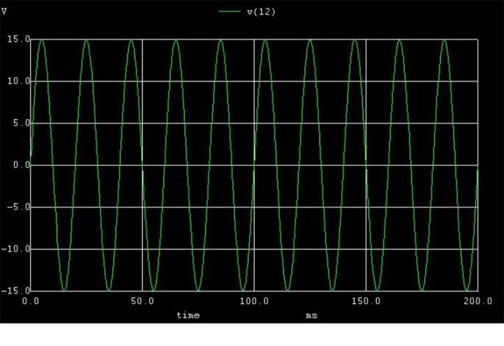
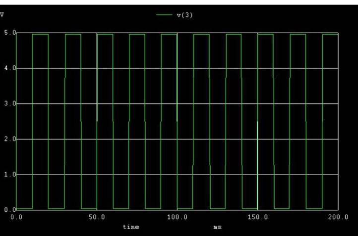
Output waveform
Schmitt trigger code:
.include timer1.cir
x1 0 2 3 5 9 2 7 5 TLC555
r1 5 0 1k
r2 2 0 10k
c1 1 2 20u
c2 9 0 0.01u
vin 1 0 sin(0 15 50)
vcc 5 0 dc 5v
.control
tran 0.5m 200m
run
plot v(1)
plot v(3)
.endc
.end