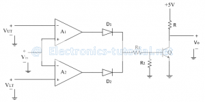
The following circuit diagram shows the window detector or window comparator using op-amp.
Operation:
Case I:Vin<VLT & Vin<VUT
With the above two conditions, output of op-amp A1 is negative (i.e. -Vsat) which will make the diode D1 reverse biased. Similarly output of op-amp A2 is positive (i.e. +Vsat) which will make the diode D2 forward biased. The positive voltage, +Vsat is now applied through potential divider formed by resistance R1 and R2 to a base of transistor Q. Due to the positive voltage at base the npn transistor Q moves into the saturation. Thus the output voltage is zero.
Thus upto VLT output voltage is zero.
Case II:Vin>VLT & Vin>VUT
With the above two conditions, output of op-amp A1 is positive (i.e. +Vsat) which will make the diode D1 forward biased. Similarly output of op-amp A2 is negative (i.e. -Vsat) which will make the diode D2 reverse biased.
The positive voltage, +Vsat is now applied through potential divider formed by resistance R1 and R2 to a base of transistor Q. Due to the positive voltage at base the npn transistor Q moves into the saturation. Thus the output voltage is zero.
Thus above VUT output voltage is zero.
Case III:VLT<Vin<VUT
With this combined condition, both the op-amps A1 and A2 goes into negative saturation (i.e. -Vsat). Both the diodes are reverse biased. So there is no voltage applied for transistor Q. Thus transistor is in cut-off and there no collector current and hence no drop across resistance R. Thus the output voltage is
∴Vo=+5V
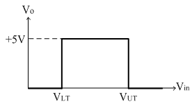
Thus between VLT and VUT (window of two voltages) output voltage is high i.e. +5V and outside this window it is zero. Therefore the circuit is called as a window detector or comparator.
The transfer characteristic of such a window comparator is shown below.
Practical example:
If we use unregulated +5V dc supply. Suppose supply goes above 5.5V some TTL circuits gets damaged. If it goes below 4.5V, the circuit is not operated properly. So with the supply 4.5V to 5.5V, the circuit can work better otherwise set off. In this case VLT = 4.5V and VUT = 5.5V
Disadvantages of open loop comparator:
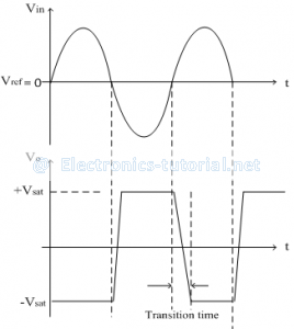
In comparators, ideally the transition from one state to another state should be instant; but practically it will take certain time to switch from one state to another state as shown in figure below.
There are slanted edges observed at the transitions. These transitions are more noticeable at high frequencies or even greater than the input signal period itself. Thus there is upper limit of the operating frequency for the comparator (i.e. max input frequency has to be considered).
This maximum operating frequency is dependent on the slew rate of the op-amp. Higher the slew rate, higher is the operating frequency.
In comparator applications, op-amp is operated in open loop configuration, so frequency compensation is not required. Thus uncompensated op-amps are preferred in comparator applications.
Since the output of op-amp goes into saturation; there are some compatibility problems with the comparator. The saturation voltage is high(= 0.9VCC). For e.g. With TTL logic,two levels are defined: +5V (logic 1) and 0V (logic 0). Thus to get the output level within specified limit, additional components are required like zener diodes.


