1. Frequency Multiplier:
In this application, the loop is broken and a frequency divider network is inserted between VCO and phase detector as shown in figure below.
Since the output of frequency divider is locked to input frequency fin, the VCO is actually running at a multiple of the input frequency. The desired amount of multiplication can be obtained by selecting a proper ÷N network.
∴Input to phase detector, fin=fo/N
∴fo=Nfin
First adjust the fin range and then adjust the free running frequency fo of the VCO by means of R1 and C1.
Consider the following example shown below. Between pin no.4 and 5 the loop is broken i.e. ÷N network is inserted. In this case we have connected IC 7490 as ÷5 network.
The output of VCO at pin no. 4 is not sufficient to drive IC so a transistor is used in-between to increase the drive. Transistor is in CE configuration so there is current gain at collector to drive IC. After ÷5 network, the frequency is applied to phase detector.
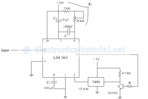
VCO frequency can be varied with the help of R1 (consists of 20kΩ pot and 2kΩ resistor) and C1.
f(Omin )=0.3/(R_(1_max ) C_1 )=0.3/(22kΩ×0.01μf )=1.3636kHz
f(Omax )=0.3/(R_(1_min ) C_1 )=0.3/(2kΩ×0.01μf )=15kHz
Thus the output frequency can be varied from 1.3636 kHz to 15 kHz with a single capacitor. The input waveform can be square wave (pin no.3) or sine wave (pin no. 2). A small capacitor, typically 1000pf is connected between pin no. 7 and 8 to eliminate possible oscillations. Also capacitor C2 should be large enough to stabilize the VCO frequency.
2. Frequency Translator (frequency Synthesizer):
In some applications we want to shift the input frequency (fin) by a small amount and not by multiple numbers. This shift is called as frequency translation (fT). It is useful in communication systems.
While transmission, a carrier frequency is used which is highly stable. We can generate carrier frequency from oscillator. For this purpose a quartz crystal oscillator is required.As crystal oscillators have some temperature coefficient, we get some thermal drift in frequency. To avoidthis frequency change due to temperature, we have to keep temperature constant. This method is very costly.
If we want to use many carrier frequencies then it is impossible to use separate crystal for each carrier frequency. So by using PLL we can generate different carrier frequencies shifted by small amount from reference frequency.
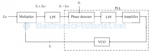
A stable frequency generated by crystal is called reference frequency and numbers of other frequencies are generated from PLL. Since the PLL IC is available in low cost, the system is not costly. The following figure shows the block diagram of frequency translator.
Externally multiplier (or mixer) and LPF are added. Multiplier is basically a non-linear circuit. Input for multipliers are fref and VCO frequency fo.
Let fref is 1 MHz and we want to shift it to a value 1.2 MHz So there is a frequency translation of 0.2 MHz.
At the output of multiplier, we have number of frequency components including addition and difference frequencies i.e. (fo ± fref). This frequency is passed through LPF. The output of LPF is the difference signal i.e. (fo-fref).
The external frequency (translation frequency) is selected such that it is equal to translation required. In the above example fT = 0.2 MHz.
Thus to achieve the locked condition, the two input frequencies for phase detector must be equal.
∴fo-fref=fT
∴fo=fT+fref
∴fo=fT+fref
∴fo=(0.2+1)MHz
∴fo=1.2 MHz
Thus the reference frequency is shifted from 1 MHz to 1.2 MHz and when the locked condition is achieved, this output frequency is highly stable i.e. translated frequency is also stable. Thus by using PLL, from a single reference frequency we can generate number of stable frequencies by this method of translation.
The instrumentation which generates number of frequencies from single reference frequency is called frequency synthesizer.
3. FM Detector:
There is shift in carrier frequency about the mean value according to modulating signal at FM transmitter. The deviation or shift in carrier frequency from centre value is converted to low voltage or high voltage, is demodulation.
Assume the loop is in locked condition, so VCO frequency and input frequency is same. FM signal is applied as input to phase detector. Phase detector produce error voltage proportional to frequency shift. This signal is passed through LPF and amplifier to give controlled voltage. Thus controlled voltage is proportional to change in frequency. As input frequency is shifted up or down, VCO voltage also varies accordingly.
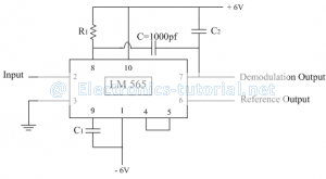
FM input is applied to pin no. 2 which is input to phase detector internally. Pin no. 4 and 5 are shorted externally to complete the loop. Initially loop is locked onto carrier frequency. As carrier frequency changes we get demodulated output at pin no.7. R1 and C1 connected externally, determine the oscillator frequency. An external capacitor of 1000pf is connected for stability of internal circuit.
Range of R1 is from 2kΩ to 20kΩ (typically=4kΩ). Direct coupling can be used at input if the dc resistance as seen from pin no. 2 and pin no. 3 are equal and if there is no dc voltage difference these two pins. If resistance is connected between pin no.6 and pin no.7, the gain of output stage can be reduced. The lock range is thus decreased with little change in VCO free running frequency
4. FSK Demodulator:
Two frequencies are used instead of two voltage levels while transmitting signal called FSK modulation. At receiver from these two frequencies we can detect the two voltage levels called FSK demodulation.
In computer peripherals and radio communication binary data or code is transmitted by means of a carrier frequency which is shifted between two predetermined frequencies. The frequencies corresponding to logic 1 and logic 0 states are commonly called as mark and space frequencies. Several standards are used to set the mark and space frequencies. For e.g.when transmitting teletypewriter information using a modem system 1070/1270 Hz pair represents the original signal and the other pair 2025/2225Hz is used as answering unit.
The difference between FSK signals of 1070 and 1270 Hz is 200 Hz and between 2025 and 2225 Hz is also 200 Hz. This is called as frequency shift. Generally binary data is transmitted at the rate of 150 Hz. At receiver end we have to generate two different voltage levels (high & low). The following figure shows the PLL IC 565 as FSK demodulator.
Pin no.4 and pin no.5 shorted externally to get VCO output to phase detector. At pin no.7 the demodulated output is available. This demodulated output is further passed through a 3 identical sections of ladder RC LPF. At the output of 3 LPF sections we get almost a dc voltage. The following figure shows the PLL IC 565 as FSK demodulator.
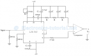
This dc voltage is applied to inverting terminal of open loop comparator. At pin no.6 reference dc voltage is present, this is second input to comparator i.e. this is the triggering point for comparator. At pin no.6 we may use RC LPF to get pure dc output.
Corresponding to 1070 Hz frequency, we get one signal VC1 at output of 3 RC LPF sections which is connected to comparator. When input frequency is shifted to 1270 Hz, we have another voltage Vc2. The triggering voltage of the comparator is adjusted such that it lies between Vc1 and Vc2. When Vc1 is received at output which is less than VT, then output of comparator is +Vsat. When Vc2 is received at output is more than VT, output of comparator changes to –Vsat.
Thus the corresponding two frequencies are converted into two voltage levels +Vsatand –Vsat (high & low) at output; which is nothing but FSK demodulation.
5. AM Detector:
The PLL can be used as an AM detector for demodulating the amplitude modulated signals.
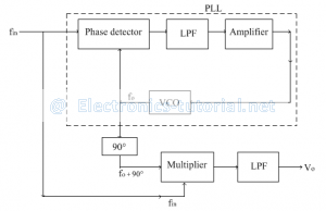
The following figure shows AM detection using PLL.
The equation of AM signal is, E[1+m cosωm t]cosωc t
where m→Modulation index (0 to 1)
ωm=2πfm→Modulating frequency
ωc=2πfc→Carrier frequency
Amplitude of VCO is constant =Ecosωc t
These are the two inputs to the multiplier block. The output is the product of the two inputs as calculated below.
=E[1+m cosωmt]cosωc t [E cosωc t]
=E^2 [1+m cosωm t] cos^2 ωc t
=E^2 [1+m cosωm t][(1+cos2ωc t)/2]
Where cos2ωc t〗 →Second harmonics of carrier frequency
When this output signal is passed through LPF, second harmonic is removed.

