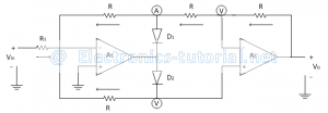
By modifying the Precision Full Wave Rectifier circuit, we get some gain for PFWR. The following circuit diagram shows the modified Precision Full Wave Rectifier.
In positive half cycle of applied ac input signal, output of op-ampA1 is negative. so diode D2 is reversed biased. Thus op-amp A1 works as an inverting amplifier with gain=(-R/R1 )
Therefore voltage at point 'A' (output of op-amp A1) is given as
VA=(-R/R1 ) Vin
The non-inverting terminal of op-amp A2 is also virtually grounded, so op-amp A2 also works as an inverting amplifier. Therefore the output voltage Vo is given as
∴Vo=-R/R [-R/R1 Vin ]
∴Vo=(R/R1 ) Vin
In negative half cycle of applied ac input signal, output of op-amp A1 is positive .so diode D2 is forward biased and diode D1 is reverse biased. Thus op-amp A1 works as an inverting amplifier.
Let V is the output of op-amp A1.
The current flowing through feedback path of op-amp A2& A1 is given as
(Vo-V)/R=(V-0)/2R
∴Vo=V/2+V
∴Vo=V[1/2+1]
∴V= 2/3 Vo
Applying KCL at node present at inverting terminal of op-amp A1, we get
(Vin-0)/R1 +(V-0)/R+(V-0)/2R=0
Vin/R1 +V/R+V/2R=0
Vin/R1 +V[1/R+1/2R]=0
Substituting the equation of 'V' in above equation as follows
Vin/R1 +2/3 Vo [(2R+R)/(2R)R]=0
Vin/R1 +2/3 Vo [3R/(2R)R]=0
Vin/R1 +2/3 Vo [3/((2R) )]=0
Vin/R1 +Vo/R=0
∴Vo=-(R/R1 ) Vin
But in negative half cycle input magnitude is negative therefore we get,
∴Vo=-(R/R1 )(-Vin )
∴Vo=(R/R1 ) Vin
Thus in both the half cycles of applied ac input signal, output remains same with gain (R/R1 )
