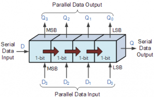
The Shift Register is another type of sequential logic circuit that can be used for the storage or the transfer of data in the form of binary numbers. This sequential device loads the data present on its inputs and then moves or “shifts” it to its output once every clock cycle, hence the name “shift register”.
A shift register basically consists of several single bit “D-Type Data Latches”, one for each data bit, either a logic “0” or a “1”, connected together in a serial type daisy-chain arrangement so that the output from one data latch becomes the input of the next latch and so on.
Data bits may be fed in or out of a shift register serially, that is one after the other from either the left or the right direction, or all together at the same time in a parallel configuration.
The number of individual data latches required to make up a single Shift Register device is usually determined by the number of bits to be stored with the most common being 8-bits (one byte) wide constructed from eight individual data latches. Shift Registers are used for data storage or for the movement of data and are therefore commonly used inside calculators or computers to store data such as two binary numbers before they are added together, or to convert the data from either a serial to parallel or parallel to serial format. The individual data latches that make up a single shift register are all driven by a common clock ( Clk ) signal making them synchronous devices. Shift register IC’s are generally provided with a clear or reset connection so that they can be “SET” or “RESET” as required.
Generally, shift registers operate in one of four different modes with the basic movement of data through a shift register being:
• Serial-in to Parallel-out (SIPO) – the register is loaded with serial data, one bit at a time, with the stored data being available at the output in parallel form.
• Serial-in to Serial-out (SISO) – the data is shifted serially “IN” and “OUT” of the register, one bit at a time in either a left or right direction under clock control.
• Parallel-in to Serial-out (PISO) – the parallel data is loaded into the register simultaneously and is shifted out of the register serially one bit at a time under clock control.
• Parallel-in to Parallel-out (PIPO) – the parallel data is loaded simultaneously into the register, and transferred together to their respective outputs by the same clock pulse.
The effect of data movement from left to right through a shift register can be presented graphically as,
Also, the directional movement of the data through a shift register can be either to the left, (left shifting) to the right, (right shifting) left-in but right-out, (rotation) or both left and right shifting within the same register thereby making it bidirectional.
